Freescale SMeCm33i3c89onductor, Inc.
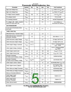
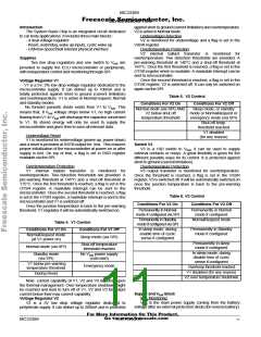
Parameter
Symbol
Min
Typ
Max
Unit
Test Conditions
TX Permanent Dominant
Timer Disable Time
BusNormal Mode and
Failure Mode
Ttxd
0.75
4
ms
TX, MOSI, SCK, CSB
High Level Input Voltage
0.7V1
V1+0.3V
SBC in Sleep Mode,
V1<1.5V
CSB Threshold for SPI Wake-up
2.2
V
CSB Filter Time for SPI Wake-up
Low Level Input Voltage
High Level Input Current on CSB
Low Level Input Current (CSB)
TX High Level Input Current
TX Low Level Input Current
SI, SCK Input Current
3
0.3 V1
-20
µs
V
SBC in Sleep Mode, V1<1V
-0.3
-100
-100
-200
-800
-10
µA
µA
µA
µA
µA
Vi=4V
Vi=1V
-20
ITX
ITX
-80
-25
Vi=4V
-320
-100
10
Vi=1V
0<VIN<V1
RX, INTB, MISO
High Level Output Voltage
Low Level Output Voltage
Tristated SO Output Current
RSTB Pin
Voh
Vol
Iz
V1-0.9
V1
0.9
+2
V
V
I0=-250µA
I0=1.5mA
0
-2
µA
0V<Vso<V1
High Level Input Voltage
Low Level Input Voltage
High Level Output current 1
High Level Output current 2
Low Level Output Voltage (I0=1.5mA)
Reset Duration after V1High
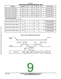
L0, L1, L2 WAKE-UP INPUTS
Positive Switching Threshold
Negative Switching Threshold
Hysteresis
Vih
Vil
0.7V1
-0.3
V1+0.3V
0.3V1
-10
V
-50
-30
µA
µA
V
0<Vout<0.5V1
0.5<Vout<V1
1v<Vbat<27V
-300
0
0.9
tres
1
ms
Vwup
Vwun
Vhyst
3
3.7
3
4.5
3.8
V
V
6V<Vbat<16V
6V<Vbat<16V
6V<Vbat<16V
2.5
700
mV
µA
µs
µA
Leakage Current 0<Vwu<Vbat
Wake up Filter Time
-5
8
+5
38
20
Lx input current @ 40V
Vin
350
600
DIGITAL INTERFACE TIMING
SCLK Clock Period
tpSCLK
500
ns
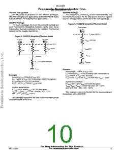
For More Information On This Product,
MC33389
MOTOROLA
7
Go to: www.freescale.com

 MOTOROLA [ MOTOROLA ]