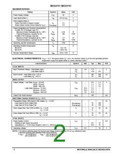
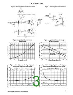
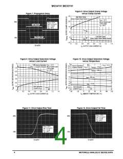
MC34151 MC33151
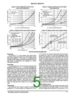
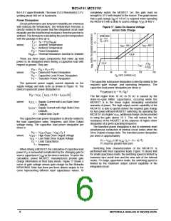
Figure 22. Controlled MOSFET Drive
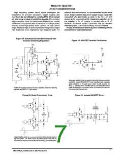
Figure 23. Bipolar Transistor Drive
V
I
B
in
V
in
+
0
–
+
Base Charge
Removal
R
g(on)
+
C
1
R
g(off)
In noise sensitive applications, both conducted and radiated EMI can
be reduced significantly by controlling the MOSFET’s turn–on and
turn–off times.
The totem–pole outputs can furnish negative base current for enhanced
transistor turn–off, with the addition of capacitor C .
1
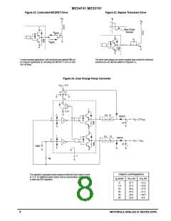
Figure 24. Dual Charge Pump Converter
V
= 15 V
CC
4.7 0.1
+
6
+
–
+
+
+
5.7V
+
+
6.8 10
1N5819
7
5
+
2
+ V
≈ 2.0 V
CC
O
+
47
+
6.8
10
+
1N5819
4
– V
≈ – V
CC
O
47
+
330pF
3
10k
Output Load Regulation
The capacitor’s equivalent series resistance limits the Drive Output Current
to 1.5 A. An additional series resistor may be required when using tantalum
or other low ESR capacitors.
I
O
(mA)
+V (V)
O
–V (V)
O
0
27.7
27.4
26.4
25.5
24.6
22.6
–13.3
–12.9
–11.9
–11.2
–10.5
–9.4
1.0
10
20
30
50
8
MOTOROLA ANALOG IC DEVICE DATA

 MOTOROLA [ MOTOROLA ]