MC34151 MC33151
MAXIMUM RATINGS
Rating
Symbol
Value
20
Unit
V
Power Supply Voltage
Logic Inputs (Note 1)
V
CC
V
in
–0.3 to V
V
CC
Drive Outputs (Note 2)
A
Totem Pole Sink or Source Current
Diode Clamp Current (Drive Output to V
I
1.5
1.0
O
)
I
CC
O(clamp)
Power Dissipation and Thermal Characteristics
D Suffix SO–8 Package Case 751
Maximum Power Dissipation @ T = 50°C
Thermal Resistance, Junction–to–Air
P Suffix 8–Pin Package Case 626
P
0.56
180
W
°C/W
A
D
R
θJA
Maximum Power Dissipation @ T = 50°C
Thermal Resistance, Junction–to–Air
P
1.0
100
W
°C/W
A
D
R
θJA
Operating Junction Temperature
T
+150
°C
°C
J
Operating Ambient Temperature
MC34151
T
A
0 to +70
MC33151
–40 to +85
Storage Temperature Range
T
stg
–65 to +150
°C
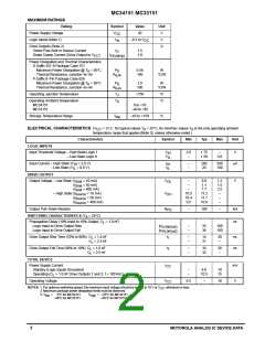
ELECTRICAL CHARACTERISTICS (V
CC
= 12 V, for typical values T = 25°C, for min/max values T is the only operating ambient
A A
temperature range that applies [Note 3], unless otherwise noted.)
Characteristics
Symbol
Min
Typ
Max
Unit
LOGIC INPUTS
Input Threshold Voltage – High State Logic 1
Input Threshold Voltage – Low State Logic 0
V
V
2.6
–
1.75
1.58
–
0.8
V
IH
IL
Input Current – High State (V = 2.6 V)
Input Current – Low State (V = 0.8 V)
IL
I
I
–
–
200
20
500
100
µA
IH
IH
IL
DRIVE OUTPUT
Output Voltage – Low State (I
Output Voltage – Low State (I
Output Voltage – Low State (I
Output Voltage – High State (I
Output Voltage – High State (I
Output Voltage – High State (I
= 10 mA)
= 50 mA)
= 400 mA)
V
–
–
–
10.5
10.4
9.5
0.8
1.1
1.7
11.2
11.1
10.9
1.2
1.5
2.5
–
–
–
V
Sink
Sink
Sink
OL
= 10 mA)
= 50 mA)
= 400 mA)
V
OH
Source
Source
Source
Output Pull–Down Resistor
R
–
100
–
kΩ
PD
SWITCHING CHARACTERISTICS (T = 25°C)
A
Propagation Delay (10% Input to 10% Output, C = 1.0 nF)
L
Logic Input to Drive Output Rise
Logic Input to Drive Output Fall
ns
t
t
–
–
35
36
100
100
PLH(in/out)
PHL(in/out)
Drive Output Rise Time (10% to 90%) C = 1.0 nF
t
–
–
14
31
30
–
ns
ns
L
r
Drive Output Rise Time (10% to 90%) C = 2.5 nF
L
Drive Output Fall Time (90% to 10%) C = 1.0 nF
t
–
–
16
32
30
–
L
f
Drive Output Fall Time (90% to 10%) C = 2.5 nF
L
TOTAL DEVICE
Power Supply Current
Standby (Logic Inputs Grounded)
I
mA
V
CC
–
–
6.0
10.5
10
15
Operating (C = 1.0 nF Drive Outputs 1 and 2, f = 100 kHz)
L
Operating Voltage
V
6.5
–
18
CC
NOTES: 1. For optimum switching speed, the maximum input voltage should be limited to 10 V or V , whichever is less.
CC
2. Maximum package power dissipation limits must be observed.
3. T
=
0°C for MC34151
–40°C for MC33151
T
= +70°C for MC34151
+85°C for MC33151
low
high
2
MOTOROLA ANALOG IC DEVICE DATA

 MOTOROLA [ MOTOROLA ]