MC34151 MC33151
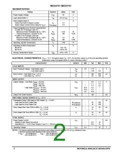
Figure 1. Switching Characteristics Test Circuit
Figure 2. Switching Waveform Definitions
12V
4.7
0.1
+
6
5.0 V
90%
Logic Input
+
–
t , t
≤ 10 ns
r
f
10%
+
0 V
+
+
t
PLH
5.7V
Drive Output
t
PHL
+
+
7
5
90%
2
4
Logic Input
10%
Drive Output
50
C
L
t
t
r
f
+
3
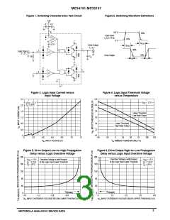
Figure 3. Logic Input Current versus
Input Voltage
Figure 4. Logic Input Threshold Voltage
versus Temperature
2.4
2.2
2.0
1.8
1.6
1.4
1.2
1.0
V
= 12 V
V
= 12 V
= 25°C
CC
CC
T
2.0
1.6
1.2
0.8
A
Upper Threshold
Low State Output
Lower Threshold
High State Output
0.4
0
0
2.0
4.0
6.0
8.0
10
12
–55
–25
0
25
50
75
C)
100
125
V
, INPUT VOLTAGE (V)
T , AMBIENT TEMPERATURE (
°
in
A
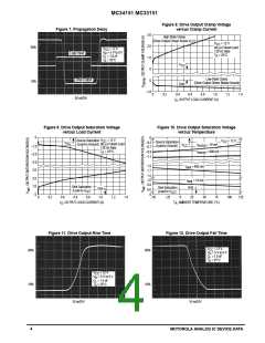
Figure 5. Drive Output Low–to–High Propagation
Delay versus Logic Overdrive Voltage
Figure 6. Drive Output High–to–Low Propagation
Delay versus Logic Input Overdrive Voltage
200
160
200
160
Overdrive Voltage is with Respect
to the Logic Input Lower Threshold
V
= 12 V
= 1.0 nF
= 25°C
Overdrive Voltage is with Respect
to the Logic Input Lower Threshold
V
= 12 V
= 1.0 nF
= 25°C
CC
L
CC
L
C
T
C
T
A
A
120
80
40
0
120
80
40
0
V
V
th(upper)
1.0
th(lower)
–1.6
–1.2
–0.8
–0.4
0
0
2.0
3.0
4.0
V
, INPUT OVERDRIVE VOLTAGE BELOW LOWER THRESHOLD (V)
V
, INPUT OVERDRIVE VOLTAGE ABOVE UPPER THRESHOLD (V)
in
in
3
MOTOROLA ANALOG IC DEVICE DATA

 MOTOROLA [ MOTOROLA ]