MC34151 MC33151
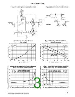
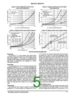
Figure 13. Drive Output Rise and Fall Time
versus Load Capacitance
Figure 14. Supply Current versus Drive Output
Load Capacitance
80
60
40
20
0
80
60
40
20
0
V
= 12 V
CC
V
V
= 12 V
CC
= 0 V to 5.0 V
Both Logic Inputs Driven
0 V to 5.0 V
IN
= 25°C
T
A
50% Duty Cycle
Both Drive Outputs Loaded
f = 200 kHz
f = 50 kHz
T
= 25°C
A
f = 500 kHz
t
f
t
r
0.1
1.0
C , OUTPUT LOAD CAPACITANCE (nF)
10
0.1
1.0
C , OUTPUT LOAD CAPACITANCE (nF)
10
L
L
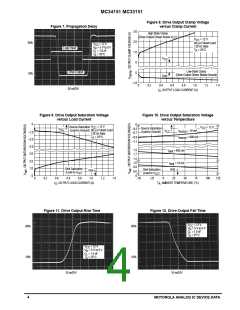
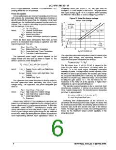
Figure 15. Supply Current versus Input Frequency
Figure 16. Supply Current versus Supply Voltage
80
8.0
6.0
4.0
2.0
T
= 25°C
Both Logic Inputs Driven
0 V to 5.0 V,
50% Duty Cycle
A
1
Logic Inputs at V
CC
60
Low State Drive Outputs
Both Drive Outputs Loaded
2
T
= 25°C
A
3
1 – V
= 18 V, C = 2.5 nF
L
CC
40 2 – V
3 – V
= 12 V, C = 2.5 nF
L
CC
CC
CC
= 18 V, C = 1.0 nF
L
4
Logic Inputs Grounded
High State Drive Outputs
4 – V
= 12 V, C = 1.0 nF
L
20
0
0
100
f, INPUT FREQUENCY (Hz)
1.0 M
10 k
0
4.0
8.0
, SUPPLY VOLTAGE (V)
12
16
V
CC
APPLICATIONS INFORMATION
Description
1.0 A. The low ‘on’ resistance allows high output currents to
be attained at a lower V than with comparative CMOS
The MC34151 is a dual inverting high speed driver
specifically designed to interface low current digital circuitry
with power MOSFETs. This device is constructed with
Schottky clamped Bipolar Analog technology which offers a
high degree of performance and ruggedness in hostile
industrial environments.
CC
drivers. Each output has a 100 kΩ pull–down resistor to keep
the MOSFET gate low when V is less than 1.4 V. No over
CC
current or thermal protection has been designed into the
device, so output shorting to V or ground must be avoided.
CC
Parasitic inductance in series with the load will cause the
driver outputs to ring above V during the turn–on transition,
CC
Input Stage
and below ground during the turn–off transition. With CMOS
drivers, this mode of operation can cause a destructive
output latch–up condition. The MC34151 is immune to output
The Logic Inputs have 170 mV of hysteresis with the input
threshold centered at 1.67 V. The input thresholds are
insensitive to V
making this device directly compatible with
latch–up. The Drive Outputs contain an internal diode to V
CC
CC
for clamping positive voltage transients. When operating with
at 18 V, proper power supply bypassing must be
CMOS and LSTTL logic families over its entire operating
voltage range. Input hysteresis provides fast output switching
that is independent of the input signal transition time,
preventing output oscillations as the input thresholds are
crossed. The inputs are designed to accept a signal
V
CC
observed to prevent the output ringing from exceeding the
maximum 20 V device rating. Negative output transients are
clamped by the internal NPN pull–up transistor. Since full
supply voltage is applied across the NPN pull–up during the
negative output transient, power dissipation at high
frequencies can become excessive. Figures 19, 20, and 21
show a method of using external Schottky diode clamps to
reduce driver power dissipation.
amplitude ranging from ground to V . This allows the output
CC
of one channel to directly drive the input of a second channel
for master–slave operation. Each input has a 30 kΩ
pull–down resistor so that an unconnected open input will
cause the associated Drive Output to be in a known high
state.
Undervoltage Lockout
Output Stage
An undervoltage lockout with hysteresis prevents erratic
system operation at low supply voltages. The UVLO forces
Each totem pole Drive Output is capable of sourcing and
sinking up to 1.5 A with a typical ‘on’ resistance of 2.4 Ω at
the Drive Outputs into a low state as V
rises from 1.4 V to
CC
5
MOTOROLA ANALOG IC DEVICE DATA

 MOTOROLA [ MOTOROLA ]