MITSUBISHI MICROCOMPUTERS
3822 Group
SINGLE-CHIP 8-BIT CMOS MICROCOMPUTER
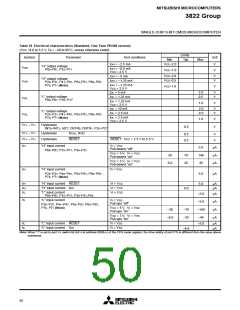
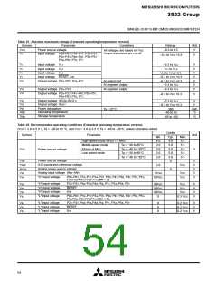
Table 23 Switching characteristics 1 (Standard, One Time PROM version)
(VCC = 4.0 to 5.5 V, VSS = 0 V, Ta = –20 to 85 °C, unless otherwise noted)
Limits
Symbol
Parameter
Unit
Min.
Typ.
Max.
140
tC (SCLK)/2–30
tC (SCLK)/2–30
ns
ns
ns
ns
ns
ns
ns
ns
twH(SCLK)
twL(SCLK)
Serial I/O clock output “H” pulse width
Serial I/O clock output “L” pulse width
td(SCLK–TXD) Serial I/O output delay time (Note 1)
–30
tv(SCLK–TXD)
tr(SCLK)
Serial I/O output valid time (Note 1)
Serial I/O clock output rising time
Serial I/O clock output falling time
CMOS output rising time (Note 2)
CMOS output falling time (Note 2)
30
30
30
30
tf(SCLK)
tr(CMOS)
tf(CMOS)
10
10
Notes 1: When the P45/TXD P-channel output disable bit of the UART control register (bit 4 of address 001B16) is “0”.
2: XOUT and XCOUT pins are excluded.
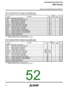
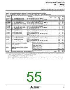
Table 24 Switching characteristics 2 (Standard, One Time PROM version)
(VCC = 2.5 to 4.0 V, VSS = 0 V, Ta = –20 to 85 °C, unless otherwise noted)
Limits
Symbol
Parameter
Serial I/O clock output “H” pulse width
Unit
Min.
Typ.
Max.
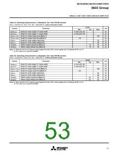
350
ns
ns
ns
ns
ns
ns
ns
ns
tC (SCLK)/2–50
tC (SCLK)/2–50
twH(SCLK)
twL(SCLK)
td(SCLK–TXD)
tv(SCLK–TXD)
tr(SCLK)
Serial I/O clock output “L” pulse width
Serial I/O output delay time (Note 1)
Serial I/O output valid time (Note 1)
Serial I/O clock output rising time
Serial I/O clock output falling time
CMOS output rising time (Note 2)
CMOS output falling time (Note 2)
–30
50
50
50
50
tf(SCLK)
tr(CMOS)
tf(CMOS)
20
20
Notes 1: When the P45/TXD P-channel output disable bit of the UART control register (bit 4 of address 001B16) is “0”.
2: XOUT and XCOUT pins are excluded.
53

 MITSUBISHI [ Mitsubishi Group ]