MITSUBISHI MICROCOMPUTERS
7477/7478 GROUP
SINGLE-CHIP 8-BIT CMOS MICROCOMPUTER
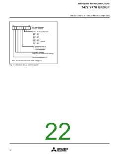
RESET CIRCUIT
Address
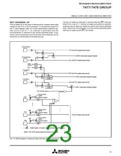
The 7477/7478 group is reset according to the sequence shown in
Figure 18. It starts the program from the address formed by using
the content of address FFFF16 as the high order address and the
content of the address FFFE16 as the low order address, when the
RESET pin is held at “L” level for no less than 2µs while the power
voltage is in the recommended operating condition and then re-
turned to “H” level.
0016
0016
0
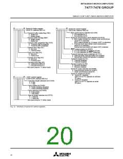
(1) Port P0 direction register
(2) Port P1 direction register
(3) Port P4 direction register
(4) P0 pull-up control register
(C116) …
(C316) …
(C916) …
(D016) …
0
0
0
0016
0
0
0
0
0
0
0
0
0
0
0
(5) P1–P5 pull-up control register (Note 1) (D116) …
The internal initializations following reset are shown in Figure 17.
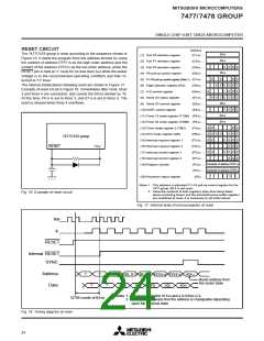
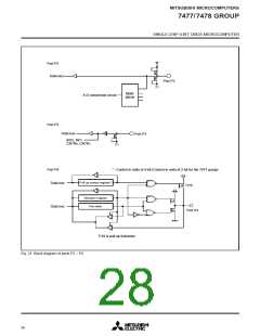
Example of reset circuit is Figure 16. Immediately after reset, timer
3 and timer 4 are connected, and counts the f(XIN) divided by 16.
At this time, FF16 is set to timer 3, and 0716 is set to timer 4. The
reset is cleared when timer 4 overflows.
0
0
0
0
1
0
0
0
0
(6) Edge selection register (EG)
(7) A-D control register
(D416) …
(D916) …
(E116) …
(E216) …
(E316) …
0
0
(8) Serial I/O status register
(9) Serial I/O control register
(10) UART control register
0016
0
0
0
0
0016
0016
(11) Timer 12 mode register (T12M) (F816) …
(12) Timer 34 mode register (T34M) (F916) …
0
0
0
0
0
0
0
0
0
0
0
0
0
0
0
0
0
0
(13) Timer mode register 2 (TM2)
(14) CPU mode register (CM)
(15) Interrupt request register 1
(16) Interrupt request register 2
(17) Interrupt control register 1
(18) Interrupt control register 2
(19) Program counter
(FA16) …
(FB16) …
(FC16) …
(FD16) …
(FE16) …
(FF16) …
(PCH) …
(PCL) …
(PS) …
0
0
0
0
0
0
0
0
7477/7478 group
RESET
VCC
0
0
0
Contents of address FFFF16
Contents of address FFFE16
1
(20) Processor status register
Notes 1 : This address is allocated P1–P4 pull-up control register for the
7477 group. Bit 6 is not used.
2 : Since the contents of both registers other than those listed
above (including timers and the transmit/receive buffer register)
are undefined at reset, it is necessary to set initial values.
Fig. 16 Example of reset circuit
Fig. 17 Internal state of microcomputer at reset
XIN
φ
RESET
Internal RESET
SYNC
Address
Data
?
?
00, S
00, S-1 00, S-2
ADH,L
FFFE16 FFFF16
Reset address from
the vector table
?
?
PCH
PCL
PS
ADL
ADH
Notes 1 : Frequency relation of XIN and φ is f(XIN)=2·φ.
32768 counts of f(XIN)
2 : The mark “?” means that the address is changeable depending
upon the previous state.
Fig. 18 Timing diagram at reset
24

 MITSUBISHI [ Mitsubishi Group ]