MITSUBISHI MICROCOMPUTERS
7477/7478 GROUP
SINGLE-CHIP 8-BIT CMOS MICROCOMPUTER
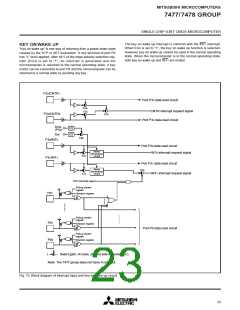
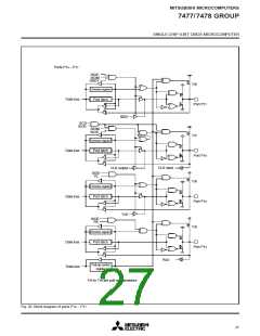
The key on wake up interrupt is common with the INT1 interrupt.
When EG5 is set to “1”, the key on wake up function is selected.
However, key on wake up cannot be used in the normal operating
state. When the microcomputer is in the normal operating state,
both key on wake up and INT1 are invalid.
KEY ON WAKE UP
“Key on wake up” is one way of returning from a power down state
caused by the STP or WIT instruction. If any terminal of port P0
has “L” level applied, after bit 5 of the edge polarity selection reg-
ister (EG5) is set to “1”, an interrupt is generated and the
microcomputer is returned to the normal operating state. A key
matrix can be connected to port P0 and the microcomputer can be
returned to a normal state by pushing any key.
P33/CNTR1
Port P33 data read circuit
EG
3
2
CNTR interrupt request signal
EG
P32/CNTR0
EG4
Port P32 data read circuit
X
CIN
(P50)
1/2
1/2
X
IN
CM
7
P3
P3
0
1
/INT
0
Port P3
0
data read circuit
interrupt request signal
Noise
eliminating
circuit
INT
0
EG
0
/INT
1
Port P31 data read circuit
Noise
eliminating
circuit
EG5
INT1 interrupt request signal
EG1
CPU halt state signal
Pull-up control
register
P0
7
Direction register
Pull-up control
register
P0
P0
1
0
Direction register
Port P0 data read circuit
Pull-up control
register
Direction register
(
Select gate: At reset, shaded side is connected.).
Note: The 7477 group does not have XCIN input.
Fig. 15 Block diagram of interrupt input and key on wake up circuit
23

 MITSUBISHI [ Mitsubishi Group ]