MITSUBISHI MICROCOMPUTERS
7477/7478 GROUP
SINGLE-CHIP 8-BIT CMOS MICROCOMPUTER
SERIAL I/O
Clock Synchronous Serial I/O Mode
Serial I/O can be used as either clock synchronous or asynchro-
nous (UART) serial I/O. A dedicated timer (baud rate generator) is
also provided for baud rate generation.
Clock synchronous serial I/O mode can be selected by setting the
mode selection bit of the serial I/O control register to “1”.
For clock synchronous serial I/O, the transmitter and the receiver
must use the same clock. If an internal clock is used, transfer is
started by a write signal to the transmit or receive buffer.
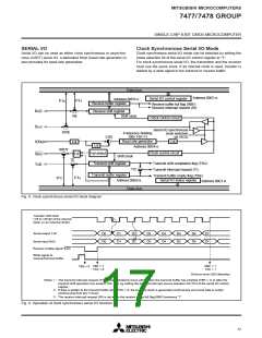
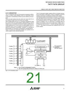
Data bus
Address 00E216
Serial I/O control register
Address 00E016
Receive buffer register
P1
4
P1
6
Receive buffer full flag (RBF)
Receive interrupt request (RI)
Receive shift register
Shift clock
RXD
RE
Clock control circuit
S
CLK
Serial I/O synchronous
SIOE
Frequency dividing
ratio 1/(n+1)
clock selection
CSS
bit (SCS)
Baud rate generator
Address 00E416
1/4
f(XIN
)
1/4
1/4
Fall detect
SRDY
Clock control circuit
S
RDY
F/F
TE
Shift clock
Transmit shift completion flag (TSC)
Transmit interrupt request (TI)
Transmit buffer empty flag (TBE)
Transmit shift register
TXD
TIC
Transmit buffer register
P1
5
P1
7
Address 00E016
Data bus
Serial I/O status register
Address 00E116
Fig. 8 Clock synchronous serial I/O block diagram
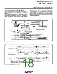
Transfer shift clock
(1/8 to 1/8192 of the internal
clock, or an external clock)
Serial output TxD
D0
D0
D1
D1
D2
D2
D3
D3
D4
D4
D5
D5
D6
D6
D7
D7
Serial input RxD
Receive enable signal SRDY
Write signal to
receive/transmit buffer
TBE = 1
TSC = 0
RBF = 1
TSC = 1
TBE = 0
Overrun error (OE) detection
Notes 1 : The transmit interrupt request (TI) can be selected to occur either when the transmit buffer has emptied (TBE = 1) or after the
transmit shift operation has ended (TSC = 1), by setting the transmit interrupt source selection bit (TIC) of the serial I/O control
register.
2 : If data is written to the transmit buffer when TSC = 0, the transmit clock is generated continuously and serial data is output
continuously from the TxD pin.
3 : The receive interrupt request (RI) is set when the receive buffer full flag (RBF) becomes “1”.
Fig. 9 Operation of clock synchronous serial I/O function
17

 MITSUBISHI [ Mitsubishi Group ]