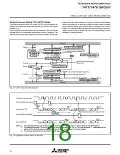
MITSUBISHI MICROCOMPUTERS
7477/7478 GROUP
SINGLE-CHIP 8-BIT CMOS MICROCOMPUTER
width or “L” width to be measured can be specified by the status of
bit 2 (CNTR0) and bit 3 (CNTR1) in the edge polarity selection reg-
ister.
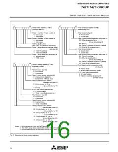
INPUT LATCH FUNCTION
The 7477/7478 group can latch the P30/INT0, P31/INT1, P32/
CNTR0, and P33/CNTR1 pin level into the input latch register (ad-
dress 00D616) when timer 4 overflows. The polarity of each pin
latched to the input latch register can be selected by using the
edge polarity selection register.
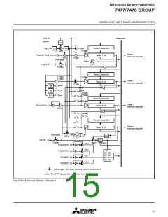
(5) PWM mode
The PWM mode can be entered for timer 3 and timer 4 by setting
bit 7 in the timer mode register 2 to “1”. In the PWM mode, the P13
pin is set for timer output T1 to output PWM waveforms by setting
bit 7 in the timer 34 mode register to “1”. The direction register of
P13 must be set for the output mode before this can be done.
In the PWM mode, timer 3 is counting and timer 4 is idle while the
PWM waveform is “L”. When timer 3 overflows, the PWM wave-
form goes “H”. At this time, timer 3 stops counting simultaneously
and timer 4 starts counting. When timer 4 overflows, the PWM
waveform goes “L”, and timer 4 stops and timer 3 starts counting
again. Consequently, the “L” duration of the PWM waveform is de-
termined by the value of timer 3; the “H” duration of the PWM
waveform is determined by the value of timer 4.
When bit 0 in the edge polarity selection register is “0”, the in-
verted value of the P30/INT0 pin level is latched; when the bit is
“1”, the P30/INT0 pin level is latched as it is.
When bit 1 in the edge polarity selection register is “0”, the in-
verted value of the P31/INT1 pin level is latched; when the bit is
“1”, the P31/INT1 pin level is latched as it is. When bit 2 in the
edge polarity selection register is “0”, the inverted value of the
P32/CNTR0 pin level is latched; when the bit is “1“, the P32/CNTR0
pin level is latched as it is. When bit 3 in the edge polarity selec-
tion register is “0”, the inverted value of the P33/CNTR1 pin level is
latched; when the bit is “1”, the P33/CNTR1 pin level is latched as
it is.
When a value is written to the timer in operation during the PWM
mode, the value is only written to the timer latch, and not written to
the timer. In this case, if the timer overflows, a value one less the
value in the timer latch is written to the timer. When any value is
written to an idle timer, the value is written to both the timer latch
and the timer.
In this mode, do not select timer 3 overflow as the count source for
timer 4.
14

 MITSUBISHI [ Mitsubishi Group ]