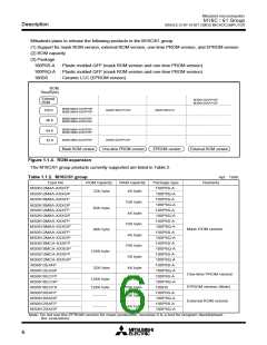
Mitsubishi microcomputers
M16C / 61 Group
SINGLE-CHIP 16-BIT CMOS MICROCOMPUTER
Memory
Operation of Functional Blocks
The M16C/61 group accommodates certain units in a single chip. These units include ROM and RAM to
store instructions and data and the central processing unit (CPU) to execute arithmetic/logic operations.
Also included are peripheral units such as timers, serial I/O, D-A converter, DMAC, CRC calculation circuit,
A-D converter, and I/O ports.
The following explains each unit.
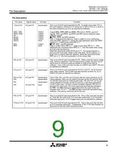
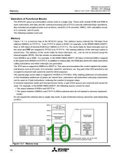
Memory
Figure 1.4.1 is a memory map of the M16C/61 group. The address space extends the 1M bytes from
address 0000016 to FFFFF16. From FFFFF16 down is ROM. For example, in the M30612M4A-XXXFP,
there is 32K bytes of internal ROM from F800016 to FFFFF16. The vector table for fixed interrupts such as
_______
the reset and NMI are mapped to FFFDC16 to FFFFF16. The starting address of the interrupt routine is
stored here. The address of the vector table for timer interrupts, etc., can be set as desired using the
internal register (INTB). See the section on interrupts for details.
From 0040016 up is RAM. For example, in the M30612M4A-XXXFP, 4K bytes of internal RAM is mapped
to the space from 0040016 to 013FF16. In addition to storing data, the RAM also stores the stack used when
calling subroutines and when interrupts are generated.
The SFR area is mapped to 0000016 to 003FF16. This area accommodates the control registers for periph-
eral devices such as I/O ports, A-D converter, serial I/O, and timers, etc. Any part of the SFR area that is not
occupied is reserved and cannot be used for other purposes.
The special page vector table is mapped to FFE0016 to FFFDB16. If the starting addresses of subroutines
or the destination addresses of jumps are stored here, subroutine call instructions and jump instructions
can be used as 2-byte instructions, reducing the number of program steps.
In memory expansion mode and microprocessor mode, a part of the spaces are reserved and cannot be
used. For example, in the M30612M4A-XXXFP, the following spaces cannot be used.
• The space between 0140016 and 03FFF16
• The space between D000016 and F7FFF16 (When external area do not expand in memory expansion
mode)
Do not expand the external area in single chip mode. A part of internal memory cannot be used depending
on MCU.
0000016
SFR area
For details, see Figure
1.7.1 and Figure 1.7.2
FFE0016
0040016
Internal RAM area
Special page
vector table
XXXXX16
Internal reserved
area (Note 1)
0400016
FFFDC16
Undefined instruction
External area
Overflow
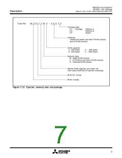
Type No.
Address XXXXX16 Address YYYYY16
BRK instruction
Address match
Single step
M30610M8A
M30610MAA
M30610MCA/EC
M30612M4A/E4
M30612M8A
M30612MAA
M30612MCA
02BFF16
02BFF16
02BFF16
013FF16
013FF16
013FF16
017FF16
F000016
E800016
E000016
F800016
F000016
E800016
E000016
Internal reserved
area (Note 2)
D000016
Watchdog timer
YYYYY16
DBC
NMI
Reset
Internal ROM area
FFFFF16
FFFFF16
Note 1: During memory expansion and microprocessor modes, can not be used.
Note 2: When external area do not expand in memory expansion mode.
Figure 1.4.1. Memory map
10

 MITSUBISHI [ Mitsubishi Group ]