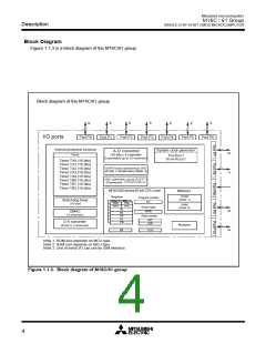
Mitsubishi microcomputers
M16C / 61 Group
SINGLE-CHIP 16-BIT CMOS MICROCOMPUTER
Pin Description
Pin Description
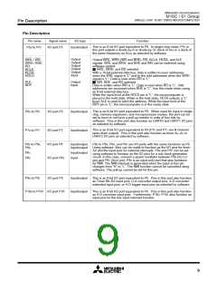
Pin name
VCC, VSS
Signal name
I/O type
Function
Power supply
input
Supply 2.7 to 5.5 V to the VCC pin. Supply 0 V to the VSS pin.
CNVSS
RESET
CNVSS
Input
This pin switches between processor modes. Connect it to the
VSS pin when operating in single-chip or memory expansion mode.
Connect it to the VCC pin when in microprocessor mode.
Reset input
Input
A “L” on this input resets the microcomputer.
XIN
Clock input
Input
These pins are provided for the main clock generating circuit.Connect
a ceramic resonator or crystal between the XIN and the XOUT pins. To
use an externally derived clock, input it to the XIN pin and leave the
XOUT pin open.
XOUT
Clock output
Output
This pin selects the width of an external data bus. A 16-bit width is
selected when this input is “L”; an 8-bit width is selected when this
input is “H”. This input must be fixed to either “H” or “L”. When
operating in single-chip mode,connect this pin to VSS.
BYTE
External data Input
bus width
select input
AVCC
AVSS
Analog power
supply input
This pin is a power supply input for the A-D converter. Connect this
pin to VCC.
Analog power
supply input
This pin is a power supply input for the A-D converter. Connect this
pin to VSS.
VREF
Input
Reference
voltage input
This pin is a reference voltage input for the A-D converter.
This is an 8-bit CMOS I/O port. It has an input/output port direction
register that allows the user to set each pin for input or output
individually. When used for input in single-chip mode, the port can be
set to have or not have a pull-up resistor in units of four bits by
software. In memory expansion and microprocessor modes, selection
of the internal pull-resistor is not available.
P00 to P07
I/O port P0
Input/output
D0 to D7
Input/output When set as a separate bus, these pins input and output data (D0–D7).
Input/output This is an 8-bit I/O port equivalent to P0.
P10 to P17
I/O port P1
I/O port P2
D8 to D15
Input/output When set as a separate bus, these pins input and output data (D
8–D15).
P20 to P27
A0 to A7
Input/output This is an 8-bit I/O port equivalent to P0.
Output
These pins output 8 low-order address bits (A0–A7).
Input/output If the external bus is set as an 8-bit wide multiplexed bus, these pins
input and output data (D0–D7) and output 8 low-order address bits
(A0–A7) separated in time by multiplexing.
A0/D0 to
A7/D7
Output
Input/output
If the external bus is set as a 16-bit wide multiplexed bus, these pins
input and output data (D0–D6) and output address (A1–A7) separated
in time by multiplexing. They also output address (A0).
A0, A1/D0
to A7/D6
P30 to P37
A8 to A15
I/O port P3
I/O port P4
Input/output This is an 8-bit I/O port equivalent to P0.
Output
These pins output 8 middle-order address bits (A8–A15).
Input/output If the external bus is set as a 16-bit wide multiplexed bus, these pins
A8/D7,
A9 to A15
Output
input and output data (D7) and output address (A8) separated in time
by multiplexing. They also output address (A9–A15).
P40 to P47
Input/output This is an 8-bit I/O port equivalent to P0.
Output
Output
These pins output CS0–CS3 signals and A16–A19. CS0–CS3 are chip
select signals used to specify an access space. A16–A19 are 4 high-
order address bits.
CS0 to CS3,
A16 to A19
8

 MITSUBISHI [ Mitsubishi Group ]