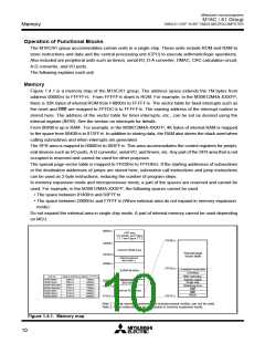
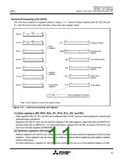
Mitsubishi microcomputers
M16C / 61 Group
SINGLE-CHIP 16-BIT CMOS MICROCOMPUTER
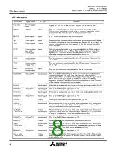
Pin Description
Pin Description
Pin name
Signal name
I/O port P5
I/O type
Function
This is an 8-bit I/O port equivalent to P0. In single-chip mode, P57 in
this port outputs a divide-by-8 or divide-by-32 clock of XIN or a clock of
the same frequency as XCIN as selected by software.
P50 to P57
Input/output
Output
Output
Output
Output
Output
Input
Output WRL, WRH (WR and BHE), RD, BCLK, HLDA, and ALE
signals. WRL and WRH, and BHE and WR can be switched using
software control.
WRL / WR,
WRH / BHE,
RD,
BCLK,
HLDA,
WRL, WRH, and RD selected
With a 16-bit external data bus, data is written to even addresses
when the WRL signal is “L” and to the odd addresses when the WRH
signal is “L”. Data is read when RD is “L”.
HOLD,
ALE,
RDY
Output
Input
WR, BHE, and RD selected
Data is written when WR is “L”. Data is read when RD is “L”. Odd
addresses are accessed when BHE is “L”. Use this mode when using
an 8-bit external data bus.
While the input level at the HOLD pin is “L”, the microcomputer is
placed in the hold state. While in the hold state, HLDA outputs a “L”
level. ALE is used to latch the address. While the input level of the
RDY pin is “L”, the microcomputer is in the ready state.
This is an 8-bit I/O port equivalent to P0. When used for input in single-
chip, memory expansion, and microprocessor modes, the port can be
set to have or not have a pull-up resistor in units of four bits by
software. Pins in this port also function as UART0 and UART1 I/O pins
as selected by software.
P60 to P67
P70 to P77
I/O port P6
Input/output
Input/output
This is an 8-bit I/O port equivalent to P6 (P70 and P71 are N channel
open-drain output). Pins in this port also function as timer A0–A3 or
UART2 I/O pins as selected by software.
I/O port P7
I/O port P8
I/O port P85
P80 to P84, P86, and P87 are I/O ports with the same functions as P6.
Using software, they can be made to function as the I/O pins for timer
A4 and the input pins for external interrupts. P86 and P87 can be set
using software to function as the I/O pins for a sub clock generation
circuit. In this case, connect a quartz oscillator between P86 (XCOUT
pin) and P87 (XCIN pin). P85 is an input-only port that also functions
for NMI. The NMI interrupt is generated when the input at this pin
changes from “H” to “L”. The NMI function cannot be cancelled using
software. The pull-up cannot be set for this pin.
P80 to P84,
P86,
Input/output
Input/output
P87,
P85
Input/output
Input
P90 to P97
I/O port P9
Input/output
Input/output
This is an 8-bit I/O port equivalent to P6. Pins in this port also function
as Timer B0–B2 input pins, D-A converter output pins, A-D converter
extended input pins, or A-D trigger input pins as selected by software.
P100 to P107 I/O port P10
This is an 8-bit I/O port equivalent to P6. Pins in this port also function
as A-D converter input pins. Furthermore, P104–P107 also function as
input pins for the key input interrupt function.
9

 MITSUBISHI [ Mitsubishi Group ]