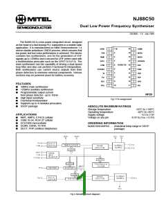
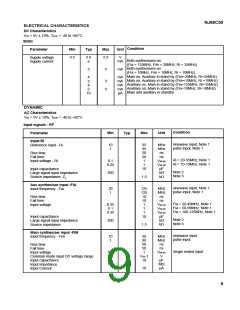
NJ88C50
ARCHITECTURE
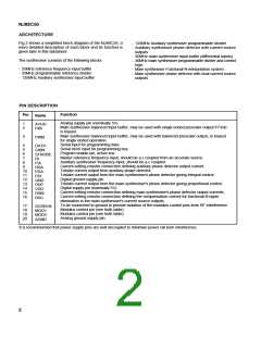
Fig.2 shows a simplified block diagram of the NJ88C50, a
more detailed description of each block and its function is
given later in this datasheet.
- 125MHz Auxiliary synthesiser programmable divider
- Auxiliary synthesiser phase detector with current source
outputs
- 30MHz main synthesiser input buffer (differential inputs)
- 30MHz main synthesiser programmable divider and control
logic
The synthesiser consists of the following blocks
- 35MHz reference frequency input buffer
- 35MHz programmable reference divider
- 125MHz Auxiliary synthesiser input buffer
- Main synthesiser Fractional-N interpolation system
- Main synthesiser phase detector with dual current source
outputs
PIN DESCRIPTION
Function
Pin
Name
Analog supply pin (nominally 5V).
Main synthesiser balanced input buffer, may be used with single ended prescaler output if Fimb
is biased.
1
2
AVDD
FIM
Main synthesiser balanced input buffer, may be used with balanced prescaler output, or biased
for single ended operation.
3
FIMB
Serial input for programming data.
Serial clock input for programming bus.
Program enable pin, active low.
Master reference frequency input, should be a.c coupled from an accurate source.
Auxiliary synthesiser frequency input, should be a.c coupled.
Current setting resistor connection defining auxiliary phase detector output current.
Tristate current output from auxiliary phase detector.
Tristate current output from the main synthesiser's phase detector giving integral control.
Digital ground supply pin.
4
5
6
7
8
9
10
11
12
13
14
15
16
DATA
CKIN
STROBE
RI
FIA
RSA
PDA
PDI
GND
PDP
VDD
RSM
RSC
Tristate current output from the main synthesiser's phase detector giving proportional control.
Digital supply pin (nominally 5V).
Current setting resistor connection defining main synthesiser's phase detector output currents.
Current setting resistor connection defining the compensation current for fractional-N ripple
elimination in the main synthesiser's current source outputs.
To be connected to ground to provide isolation of the modulus control pins from RF interference.
Modulus control pin (see truth table).
17
18
19
20
SCREEN
MOD1
MOD2
Modulus control pin (see truth table).
Analog ground supply pin.
AGND
It is recommended that power supply pins are well decoupled to minimise power rail born interference.
2

 MITEL [ MITEL NETWORKS CORPORATION ]