MT9160B/61B
Advance Information
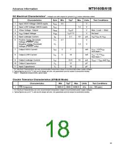
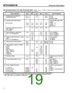
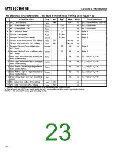
AC Characteristics† for A/D (Transmit) Path - 0dBm0 = A
- 3.17dB = 1.773V
for µ-Law and 0dBm0 = A
Lo3.14
Lo3.17
rms
- 3.14dB =1.843V
for A-Law, at the Codec (V =0.6 volts and V =2.5 volts.)
Bias
rms
Ref
‡
Characteristics
Sym
Min
Typ
Max
Units
Test Conditions
µ-Law
1
2
Analog input equivalent to
overload decision
A
7.33
7.6
Vp-p
Vp-p
Li3.17
Li3.14
A
A-Law
Both at Codec
Absolute half-channel gain
Transmit filter gain=0dB
setting.
M ± to Dout
G
G
5.2
14.5
6.0
15.3
6.8
16.1
dB
dB
TxINC = 0*
TxINC = 1*
AX1
AX2
@1020 Hz
Tolerance at all other transmit
filter settings
-0.2
±0.1
+0.2
dB
(1 to 7dB)
3
4
Gain tracking vs. input level
ITU-T G.714 Method 2
G
-0.3
-0.6
-1.6
0.3
0.6
1.6
dB
dB
dB
3 to -40 dBm0
-40 to -50 dBm0
-50 to -55 dBm0
TX
QX
CX
Signal to total Distortion vs. input
level.
ITU-T G.714 Method 2
D
N
35
29
24
dB
dB
dB
0 to -30 dBm0
-40 dBm0
-45 dBm0
5
6
Transmit Idle Channel Noise
8.5
-71
12
-69
dBrnC0 µ-Law
dBm0p A-Law
N
PX
Gain relative to gain at 1020Hz
G
RX
<50Hz
60Hz
200Hz
300 - 3000 Hz
3000 - 3400 Hz
4000 Hz
-25
-30
0.0
0.25
0.25
-12.5
-25
dB
dB
dB
dB
dB
dB
dB
-45
-0.25
-0.9
-23
-40
>4600 Hz
7
8
Absolute Delay
D
D
360
µs
at frequency of minimum
delay
AX
Group Delay relative to D
750
380
130
750
µs
µs
µs
µs
500-600 Hz
AX
DX
600 - 1000 Hz
1000 - 2600 Hz
2600 - 2800 Hz
9
Power Supply Rejection
±100mV peak signal on
V
DD
f=1020 Hz
PSSR
PSSR1
PSSR2
PSSR3
37
dB
dB
dB
dB
µ-law
f=0.3 to 3 kHz
f=3 to 4 kHz
f=4 to 50 kHz
40
35
40
PSSR1-3 not production
tested
† AC Electrical Characteristics are over recommended temperature range & recommended power supply voltages.
‡ Typical figures are at 25 °C and are for design aid only: not guaranteed and not subject to production testing.
* Note: TxINC, refer to Control Register 1, address 00h.
97

 MITEL [ MITEL NETWORKS CORPORATION ]