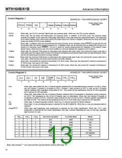
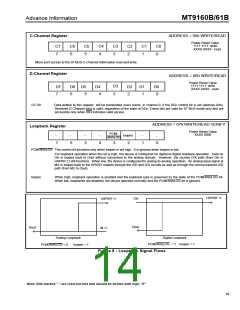
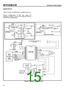
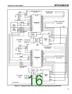
MT9160B/61B
Advance Information
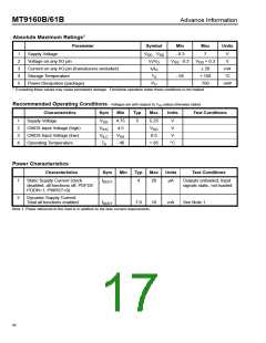
Absolute Maximum Ratings†
Parameter
Symbol
- V
Min
Max
Units
1
2
3
4
5
Supply Voltage
V
- 0.3
7
V
V
DD
SS
Voltage on any I/O pin
V /V
V
- 0.3
V
+ 0.3
DD
I
O
SS
Current on any I/O pin (transducers excluded)
Storage Temperature
I /I
± 20
+ 150
750
mA
°C
I O
T
P
- 65
S
Power Dissipation (package)
mW
D
†
Exceeding these values may cause permanent damage. Functional operation under these conditions is not implied.
Recommended Operating Conditions - Voltages are with respect to V unless otherwise stated
SS
Characteristics
Supply Voltage
Sym
Min
Typ
Max
Units
Test Conditions
1
2
3
4
V
4.75
4.5
5
5.25
V
V
DD
CMOS Input Voltage (high)
CMOS Input Voltage (low)
Operating Temperature
V
V
DD
IHC
V
V
0.5
V
ILC
SS
T
- 40
+ 85
°C
A
Power Characteristics
Characteristics
Sym
Min
Typ
Max
Units
Test Conditions
1
2
Static Supply Current (clock
disabled, all functions off, PDFDI/
PDDR=1, PWRST=0)
I
4
20
µA
Outputs unloaded, Input
signals static, not loaded
DDC1
Dynamic Supply Current:
Total all functions enabled
I
7.0
10
mA
See Note 1.
DDFT
Note 1: Power delivered to the load is in addition to the bias current requirements.
95

 MITEL [ MITEL NETWORKS CORPORATION ]