MT9076
Preliminary Information
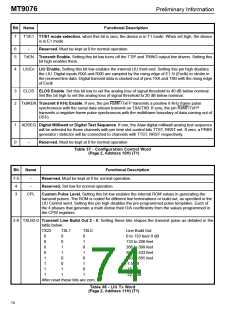
Bit Name
Functional Description
7
T1/E1 T1/E1 mode selection. when this bit is zero, the device is in T1 mode. When set high, the device
is in E1 mode.
6
5
--
Reserved. Must be kept at 0 for normal operation.
TxEN Transmit Enable. Setting this bit low turns off the TTIP and TRING output line drivers. Setting this
bit high enables them.
4
LIUEn LIU Enable. Setting this bit low enables the internal LIU front-end. Setting this pin high disables
the LIU. Digital inputs RXA and RXB are sampled by the rising edge of E1.5i (Exclk) to strobe in
the received line data. Digital transmit data is clocked out of pins TXA and TXB with the rising edge
of Exclk
3
2
ELOS ELOS Enable. Set this bit low to set the analog loss of signal threshold to 40 dB below nominal.
Set this bit high to set the analog loss of signal threshold to 20 dB below nominal.
Tx8KEN Transmit 8 KHz Enable. If one, the pin RxMF/TxFP transmits a positive 8 KHz frame pulse
synchronous with the serial data stream transmit on TXA/TXB. If zero, the pin RxMF/TxFP
transmits a negative frame pulse synchronous with the multiframe boundary of data coming out of
DSTo.
1
0
ADSEQ Digital Milliwatt or Digital Test Sequence. If one, the Alaw digital milliwatt analog test sequence
will be selected for those channels with per time slot control bits TTST, RRST set. If zero, a PRBS
generator / detector will be connected to channels with TTST, RRST respectively.
--
Reserved. Must be kept at 0 for normal operation.
Table 37 - Configuration Control Word
(Page 2, Address 10H) (T1)
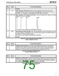
Bit
Name
Functional Description
7-5
4
--
--
Reserved. Must be kept at 0 for normal operation.
Reserved. Set low for normal operation.
3
CPL
Custom Pulse Level. Setting this bit low enables the internal ROM values in generating the
transmit pulses. The ROM is coded for different line terminations or build out, as specified in the
LIU Control word. Setting this pin high disables the pre-programmed pulse templates. Each of
the 4 phases that generate a mark derive their D/A coefficients from the values programmed in
the CPW registers.
2-0 TXLB2-0 Transmit Line Build Out 2 - 0. Setting these bits shapes the transmit pulse as detailed in the
table below:
TX22
TXL1
TXL0
Line Build Out
0 to 133 feet/ 0 dB
133 to 266 feet
266 to 399 feet
399 to 533 feet
533 to 655 feet
-7.5 dB
0
0
0
0
1
1
1
1
0
0
1
1
0
0
1
1
0
1
0
1
0
1
0
1
-15 dB
-22.5 dB
After reset these bits are zero.
Table 38 - LIU Tx Word
(Page 2, Address 11H) (T1)
70

 MITEL [ MITEL NETWORKS CORPORATION ]