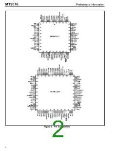
MT9076
Preliminary Information
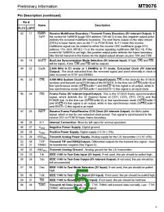
Pin Description (continued)
Pin #
Name
Description
PLCC LQFP
61
43
LOS
Loss of Signal or Synchronization (5V tolerant Output). When high, and LOS/LOF
(page 01H address 19H bit 0) is zero, this signal indicates that the receive portion of the
MT9076 is either not detecting an incoming signal (bit LLOS on page 03H address 16H
is one) or is detecting a loss of basic frame alignment condition (bit TSYNC (T1), SYNC
(E1) on page 03H address 10H is one). If LOS/LOF=1, a high on this pin indicates a
loss of signal condition.
62
63
64
44
45
IC2
IC3
Internal Connection (3V Input). Tie to V (Ground) for normal operation.
SS
Internal Connection (3V Input). Tie to V (Ground) for normal operation.
SS
46 TxDLCLK Transmit Data Link Clock (5V tolerant Output). A gapped clock signal derived from a
gated 2.048 Mbit/s clock for transmit data link at 4, 8, 12, 16 or 20 kHz. The transmit
data link data (TxDL) is clocked in on the rising edge of TxDLCLK. TxDLCLK can also
be used to clock DL data out of an external serial controller.
65
66
47
TxDL
Transmit Data Link (5V tolerant Input). An input serial stream of transmit data link
data at 4, 8, 12, 16 or 20 kbit/s.
48
S/FR/ Synchronization/ Freerun / Extracted Clock (5V tolerant Input). If low, and the
Exclki internal LIU is enabled, the MT9076 is in free run mode. Pins 45 C4b and 46 F0b are
outputs generating sytem clocks. Slips will occur in the receive slip buffer as a result of
any deviation between the MT9076's internal PLL (which is free - running) and the
frequency of the incoming line data. If high, and the internal LIU is enabled, the MT9076
is in Bus or Line Synchronization mode depending on the BS/LS pin. If the internal LIU
is disabled, in digital framer mode, this pin (Exclki) takes an input clock 1.544Mhz (T1) /
2.048Mhz (E1) that clocks in the received digital data on pins RXA and RXB with its
rising edge.
67
68
49
50
VDD3 Positive Power Supply. Digital supply (+3.3V ± 5%).
VSS3 Negative Power Supply. Digital ground.
Device Overview
The MT9076 is a T1/E1/J1 single chip transceiver that incorporates an advanced framer, a long-haul LIU (Line
Interface Unit), a low jitter PLL (Phase Locked Loop) and 3 HDLCs (High-level Data Link Controller). The T1,
E1 and J1 operating modes are selectable under software control.
Standards Compliance
In T1 mode, the MT9076 meets or supports the latest recommendations including Telcordia GR-303-CORE,
AT&T PUB43801, TR-62411, ANSI T1.102, T1.403 and T1.408. In T1 ESF mode the CRC-6 calculation and
yellow alarm can be configured to meet the requirements of a J1 interface.
In E1 mode, the MT9076 meets or supports the latest ITU-T Recommendations for PCM 30 and ISDN primary
rate including G.703, G.704, G.706, G.732, G.775, G.796, G.823, G.964 (V5.1), G.965 (V5,2) and I.431. It also
meets or supports ETSI ETS 300 011, ETS 300 166, ETS 300 233, ETS 300 324 (V5.1) and ETS 300 347
(V5.2).
Microprocessor Port
The MT9076 registers are accessible via an 8-bit parallel Motorola or Intel non-multiplexed microprocessor
interface.
6

 MITEL [ MITEL NETWORKS CORPORATION ]