MT9076
Preliminary Information
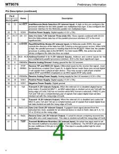
Pin Description (continued)
Pin #
Name
Description
PLCC LQFP
19
72
INT/MOT Intel/Motorola Mode Selection (5V tolerant Input). A high on this pin configures the
processor interface for the Intel parallel non-multiplexed bus type. A low configures the
processor interface for the Motorola parallel non-multiplexed type.
20
73
VDD5 Positive Power Supply. Digital supply (+3.3V ± 5%).
21 - 74-77 D4 - D7 Data 4 to Data 7 (5V tolerant Three-state I/O). These signals combined with D0-D3
24
form the bidirectional data bus of the parallel processor interface (D7 is the most
significant bit).
25
78
R/W/WR Read/Write/Write Strobe (5V tolerant Input). In Motorola mode (R/W), this input
controls the direction of the data bus D[0:7] during a microprocessor access. When R/W
is high, the parallel processor is reading data from the MT9076. When low, the parallel
processor is writing data to the MT9076. For Intel mode (WR), this active low write
strobe configures the data bus lines as output.
26 -
30
79, AC0 - AC4 Address/Control 0 to 4 (5V tolerant Inputs). Address and control inputs for the
2-5
non-multiplexed parallel processor interface. AC0 is the least significant input.
31
6
GNDARx Receive Analog Ground. Analog ground for the LIU receiver.
32
33
7
8
RTIP
Receive TIP and RING (3V Input). Differential inputs for the receive line signal - must
RRING be transformer coupled (See Figure 6). In digital framer mode these pins accept digital
3 volt signals from a physical layer device. They may accept a split phase unipolar
signal (RTIP and RRING employed) or an NRZ signal (RTIP only used).
34
35
36
37
9
VDDARx Receive Analog Power Supply. Analog supply for the LIU receiver (+3.3V ± 5%).
VDD1 Positive Power Supply. Digital supply (+3.3V ± 5%).
10
11
12
VSS1 Negative Power Supply. Digital ground.
TxA
Transmit A (5V tolerant Output). When the internal LIU is disabled (digital framer
only mode), if control bit NRZ=1, an NRZ output data is clocked out on pin TxA with the
rising edge of Exclk (TxB has no function when NRZ format is selected). If NRZ=0, pins
TxA and TxB are a complementary pair of signals that output digital dual-rail data
clocked out with the rising edge of Exclk.
38
39
13
TxB
Transmit B (5V tolerant Output). When the internal LIU is disabled and control bit
NRZ=0, pins TxA and TxB are a complementary pair of signals that output digital dual-
rail data clocked out with the rising edge of Exclk.
14 RxDLCLK Data Link Clock (5V tolerant Output). A gapped clock signal derived from the
extracted line clock, available for an external device to clock in RxDL data (at 4, 8, 12,
16 or 20 kHz) on the rising edge.
40
41
15
RxDL
Receive Data Link (5V tolerant Output). A serial bit stream containing received line
data after zero code suppression. This data is clocked out with the rising edge of Exclk.
16
TxMF Transmit Multiframe Boundary (5V tolerant Input). An active low input used to set
the transmit multiframe boundary (CAS or CRC multiframe). The MT9076 will generate
its own multiframe if this pin is held high. This input is usually pulled high for most
applications.
4

 MITEL [ MITEL NETWORKS CORPORATION ]