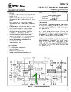
Preliminary Information
MT9076
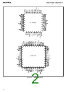
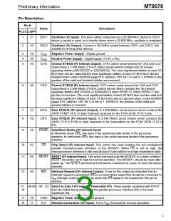
Pin Description (continued)
Pin #
Name
Description
PLCC LQFP
42
17
RxMF/ Receive Multiframe Boundary / Transmit Frame Boundary (5V tolerant Output). If
TxFP
the control bit Tx8KEN (page 02H address 10H bit 2) is low, this negative output pulse
delimits the received multiframe boundary. The next frame output on the data stream
(DSTo) is basic frame zero on the T1 or PCM 30 link. In E1 mode this receive
multiframe signal can be related to either the receive CRC multiframe (page 01H,
address 17H, bit 6, MFSEL=1) or the receive signaling multiframe (MFSEL=0). If the
control bit Tx8KEN is set high, this positive output pulse delimits the frame boundary
(the first bit transmit in the frame) for the digital output stream on pins TXA and TXB.
43
44
18
22
BS/LS Bus/Line Syncronization Mode Selection (5V tolerant Input). If high, C4b and F0b
will be inputs; if low, C4b and F0b will be outputs.
Exclk
C4b
2.048 MHz in E1 mode or 1.544MHz in T1 mode, Extracted Clock (5V tolerant
Output). The clock extracted from the received signal and used internally to clock in
data received on RTIP and RRING.
45
46
23
24
4.096 MHz System Clock (5V tolerant Input/Output). C4b is the clock for the ST-BUS
sections and transmit serial PCM data of the MT9076. In the free-run (S/FR/Exclki=0) or
line synchronous mode (S/FR/Exclki=1 and BS/LS=0) this signal is an output, while in
bus synchronous mode (S/FR/Exclki=1 and BS/LS=1) this signal is an input clock.
F0b
Frame Pulse (5V tolerant Input/Output). This is the ST-BUS frame synchronization
signal, which delimits the 32 channel frame of CSTi, CSTo, DSTi, DSTo and the
PCM30 link. In the free-run (S/FR/Exclki=0) or line synchronous mode (S/FR/Exclki=1
and BS/LS=0) this signal is an output, while in bus synchronous mode (S/FR/Exclki=1
and BS/LS=1) this signal is an input.
47
25
RxFP
IC1
Receive Frame Pulse/Receive CCS Clock (5V tolerant Output). An 8kHz pulse
signal, which is low for one extracted clock period. This signal is synchronized to the
receive DS1 or PCM 30 basic frame boundary.
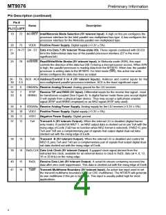
48
49
50
51
26
27
28
29
Internal Connection. Must be left open for normal operation.
Negative Power Supply. Digital ground.
V
SS2
DD2
V
Positive Power Supply. Digital supply (+3.3V ± 5%).
VDD
Transmit Analog Power Supply. Analog supply for the LIU transmitter (+3.3V ±5%).
ATx
52
53
30
31
TTIP
Transmit TIP and RING(Output). Differential outputs for the transmit line signal - must
TRING be transformer coupled (See Figure 6).
54
55
56
32
33
34
GND
Transmit Analog Ground . Analog ground for the LIU transmitter.
ATx
Tdi
IEEE 1149.1a Test Data Input (3V Input). If not used, this pin should be pulled high.
Tdo
IEEE 1149.1a Test Data Output (5V tolerant Output). If not used, this pin should be
left unconnected.
57
35
Tms
IEEE 1149.1a Test Mode Selection (3V Input). If not used, this pin should be pulled
high.
58
59
60
36
37
38
Tclk
Trst
IEEE 1149.1a Test Clock Signal (3V Input). If not used, this pin should be pulled high.
IEEE 1149.1a Reset Signal (3V Input). If not used, this pin should be held low.
TxAO
Transmit All Ones (Input). High - TTIP, TRING will transmit data normally. Low - TTIP,
TRING will transmit an all ones signal.
5

 MITEL [ MITEL NETWORKS CORPORATION ]