Preliminary Information
MT9076
6.0 Transmit Data All Ones (TxAO) Operation
The TxAO (Transmit all ones) pin allows the PRI interface to transmit an all ones signal under hardware control.
7.0 Data Link Operation
7.1
Data Link Operation in E1 mode
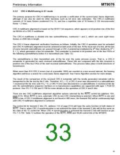
In E1 mode, MT9076 has a user defined 4, 8, 12, 16 or 20 kbit/s data link for transport of maintenance and
performance monitoring information across the PCM 30 link. This channel functions using the S bits (S ~S )
a
a4
a8
of the PCM 30 timeslot zero non-frame alignment signal (NFAS). Since the NFAS is transmitted every other
frame - a periodicity of 250 microseconds - the aggregate bit rate is a multiple of 4 kb/s. As there are five S
a
bits independently available for this data link, the bit rate will be 4, 8, 12, 16 or 20 kb/s, depending on the bits
selected for the Data Link (DL).
The S bits used for the DL are selected by setting the appropriate bits, S ~S , to one in the Data Link Select
a
a4
a8
Word (page 01H, address 17H, bits 4-0). Access to the DL is provided by pins TxDLCLK, TxDL, RxDLCLK and
RxDL, which allow easy interfacing to an external controller.
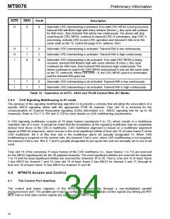
Data to be transmit onto the line in the S bit position is clocked in from the TxDL pin (pin 65 in PLCC, pin 47 in
a
LQFP) with the clock TxDLCLK (pin 64 in PLCC, pin 46 pin LQFP). Although the aggregate clock rate equals
the bit rate, it has a nominal pulse width of 244 ns, and it clocks in the TxDL as if it were a 2.048 Mb/s data
stream. The clock can only be active during bit times 4 to 0 of the STBUS frame. The TxDL input signal is
clocked into the MT9076 by the rising edge of TxDLCLK. If bits are selected to be a part of the DL, all other
programmed functions for those S bit positions are overridden.
a
The RxDLCLK signal (pin 39 - PLCC, pin 14 - LQFP) is derived from the receive extracted clock and is aligned
with the receive data link output RxDL. The HDB3 decoded receive data, at 2.048 Mbit/s, is clocked out of the
device on pin RxDL (pin 40 in PLCC, pin 15 in LQFP). In order to facilitate the attachment of this data stream to
a Data Link controller, the clock signal RxDLCLK consists of positive pulses, of nominal width of 244 ns, during
the S bit cell times that are selected for the data link.This selection is made by programming address 17H of
a
master control page 01H. No DL data will be lost or repeated when a receive frame slip occurs. See AC
Electrical Characteristics for timing requirements.
7.2
Data Link Operation in T1 mode
SLC-96 and ESF protocol allow for carrier messages to be embedded in the overhead bit position. The
MT9076 provides 3 separate means of controlling these data links. See Data Link Control Word - address 12H,
page 1H.
•
The data links (transmit and receive) may be sourced (sunk) from an external controller using dedicated
pins on the MT9076 in T1 mode (enabled by setting the bit 7 - EDL of the Data link Control Word).
•
Bit Oriented Messages may be transmit and received via a dedicated TxBOM register (page 1H,
address 13H) and a RxBOM (page 3H, address 15H). Transmission is enabled by setting bit 6 - BIOMEn
in the Data link Control Word. Bit - oriented messages may be periodically interrupted (up to once per
second) for a duration of up to 100 milliseconds. This is to accommodate bursts of message - oriented
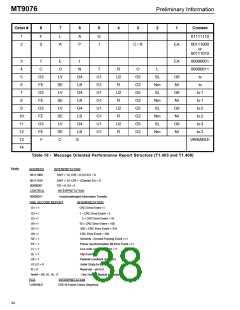
protocols. See Table 16 for message structure.
33

 MITEL [ MITEL NETWORKS CORPORATION ]