Preliminary Information
MT9076
4.2
Control and Status Register Access
The controlling microprocessor gains access to specific registers of the MT9076 through a two step process.
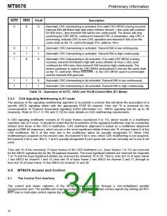
First, writing to the Command/Address Register (CAR) selects one of the 15 pages of control and status
registers (CAR address: AC4 = 0, AC3-AC0 = don't care, CAR data D7 - D0 = page number). Second, each
page has a maximum of 16 registers that are addressed on a read or write to a non-CAR address (non-CAR:
address AC4 = 1, AC3-AC0 = register address, D7-D0 = data). Once a page of memory is selected, it is only
necessary to write to the CAR when a different page is to be accessed. See the AC Electrical Characteristics
section.
Page Address D7 - D0
Register Description
Processor Access
ST-BUS Access
00000001 (01H)
00000010 (02H)
00000011 (03H)
00000100 (04H)
00000101 (05H)
00000110 (06H)
00000111 (07H)
00001000 (08H)
00001001 (09H)
00001010 (0AH)
00001011 (0BH)
00001011 (0CH)
00001011 (0DH)
00001011 (0EH)
00001011 (0FH)
Master
Control
R/W
R/W
R
- - -
Master
Status
- - -
R/W
R/W
R/W
Per Channel Transmit signaling
Per Channel Transmit signaling
Per Time Slot Control
CSTi
CSTi
- - -
- - -
CSTo
CSTo
- -
Per Time Slot Control
R/W
R/W
R/W
R/W
R/W
R/W
R/W
R
Per Channel Receive signaling
Per Channel Receive signaling
HDLC0 Control and Status
HDLC1 Control and Status
HDLC2 Control and Status
Tx National Bit Buffer
---
---
---
Rx National Bit Buffer
---
Table 13 - Page Summary
Please note that for microprocessors with read/write cycles less than 200 ns, a wait state or a dummy operation
(for C programming) between two successive read/write operations to the HDLC FIFO is required.
Table 13 associates the MT9076 control and status pages with access and page descriptions.
4.3
Identification Code
The MT9076 shall be identified by the code 01111000, read from the identification code status register (page
03H, address 1FH).
4.4
ST-BUS Streams
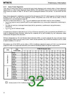
In T1 mode, there is one control and one status ST-BUS stream that can be used to program / access channel
associated signaling nibbles. CSTo contains the received channel associated signaling bits, and for those
channels whose Per Time Slot Control word bit 1 "RPSIG" is set low, CSTi is used to control the transmit
channel associated signaling. The DSTi and DSTo streams contain the transmit and receive voice and digital
data. Only 24 of the 32 ST-BUS channels are used for each of DSTi, DSTo, CSTi and CSTo. In each case
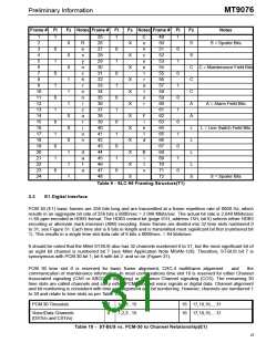
individual channel mapping is as illustrated in Table 6, “ST-BUS vs. DS1 to Channel Relationship(T1),” on
page 25.
In E1 mode, ST-BUS streams can also be used to access channel associated signaling nibbles. CSTo contains
the received channel associated signaling bits (e.g., ITU-T R1 and R2 signaling) ,and for those channels whose
31

 MITEL [ MITEL NETWORKS CORPORATION ]