MT9076
Preliminary Information
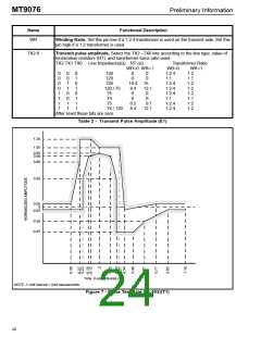
•
In Line Synchronous mode, the clock extracted from the receive data is dejittered using the internal PLL
and then output on pin C4b. Pin Exclk provides the extracted receive clock before it has been dejittered.
The transmit data is synchronous to the clean receive clock.
•
In Free-Run mode the transmit data is synchronized to the internally generated clock. The internal clock
is output on pin C4b. The clock signal extracted from the receive data is not dejittered and is output
directly on Exclk.
2.1
Jitter Attenuator FIFO
In System Bus Synchronous operation, a data buffer is required between the jittered input clock and the clean
transmit clock. In normal T1 mode, the transmit slip buffer performs this function. In T1 IMA mode, the transmit
slip buffer is unused, instead a jitter attenuator FIFO is employed. In an E1 mode System Bus Synchronous
configuration, the jitter attenuator FIFO is always used. In this case the C4b signal clocks the data into the
FIFO, the PLL de-jitters the C4b clock and the resulting clean C4b signal clocks the data out of the FIFO.
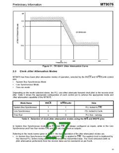
The JA meets the jitter transfer characteristics as proposed by ETSI ETS 300 011, G.735 and the relevant
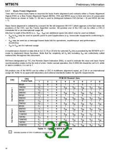
recommendations as shown in Figure 12. The JA FIFO depth can be selected to be from 16 to 128 words deep,
in multiples of 16 (2-bit) words. Its read pointer can be centered by changing the JFC bit (address 13H of page
02H) to provide maximum jitter tolerance. If the read pointer should come within 4 bits of either end of the
FIFO, the read clock frequency will be increased or decreased by 0.0625 UI to correct the situation. The
maximum time needed to centre is T
= 3904 Depth ns, where Depth is the selected JA FIFO depth. During
max
this time the JA will not attenuate jitter.
2.2
IMA Mode
2.2.1
T1 Mode
In T1 IMA Mode, neither the transmit nor the receive slip buffers are activated. Channel Associated signaling
(CAS) and HDLC operation is not supported. The input pin C4b accepts a 1.544 MHz clock and it clocks
incoming data from DSTi into a jitter attenuator FIFO. This clock is dejittered with the internal PLL. The
dejittered clock clocks data out of the FIFO for transmission onto the line. Receive clock (1.544 MHz) and data
is extracted from the line and routed to pins Exclk and DSTo respectively. The receive clock Exclk is not
dejittered before being driven off chip. For operation in IMA mode, the MT9076 should be programmed in
System Bus Synchronous mode (BS/LS and S/FR/Exclki set high).
2.2.2
E1 Mode
In E1 IMA Mode neither the transmit nor the receive slip buffers are activated. The input pin C4b accepts a
2.048 MHz clock and it clocks incoming data from DSTi into a jitter attenuator FIFO. This clock is dejittered with
the internal PLL. The dejittered clock clocks data out of the FIFO for transmission onto the line. Receive clock
(2.048 MHz) and data is extracted from the line and routed to pins Exclk and DSTo respectively. The receive
clock Exclk is not dejittered before being driven off chip. For operation in IMA mode, the MT9076 should be
programmed in System Bus Synchronous mode (BS/LS and S/FR/Exclki set high).
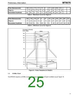
3.0 The Digital Interface
3.1
T1 Digital Interface
In T1 mode, DS1 frames are 193 bits long and are transmitted at a frame repetition rate of 8000 Hz, which
results in an aggregate bit rate of 193 bits x 8000/sec= 1.544 Mbits/sec. The actual bit rate is 1.544 Mbits/sec
+/-50 ppm optionally encoded in B8ZS format. The Zero Suppression control register (page 1, address 15H,)
selects either B8ZS encoding, forced one stuffing or alternate mark inversion (AMI) encoding. Basic frames are
divided into 24 time slots numbered 1 to 24. Each time slot is 8 bits in length and is transmitted most significant
bit first (numbered bit 1). This results in a single time slot data rate of 8 bits x 8000/sec. = 64 kbits/sec.
24

 MITEL [ MITEL NETWORKS CORPORATION ]