Preliminary Information
MT9076
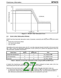
dB
-0.5
0
-20 dB/decade
19.5
10
40
400
10K
Frequency (Hz)
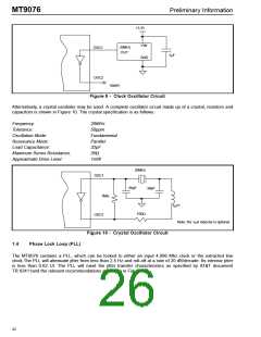
Figure 11 - TR 62411 Jitter Attenuation Curve
2.0 Clock Jitter Attenuation Modes
MT9076 has three basic jitter attenuation modes of operation, selected by the BS/LS and S/FR/Exclki control
pins.
•
•
•
System Bus Synchronous Mode
Line Synchronous Mode
Free-run mode
Depending on the mode selection above, the PLL can either attenuate transmit clock jitter or the receive clock
jitter. Table 5 shows the appropriate configuration of each control pin to achieve the appropriate mode and
Jitter attenuation capability of the MT9076.
Mode Name
BS/LS
S/FR/Exclki
Note
System Bus Synchronous
Line Synchronous
Free-Run
1
0
x
1
1
0
PLL locked to C4b.
PLL locked to Exclk.
PLL free - running.
Table 5 - Selection of clock jitter attenuation modes using the M/S and MS/FR pins
In System Bus Synchronous mode, pins C4b and F0b are always configured as inputs, while in the Line
Synchronous and Free-Run modes C4b and F0b are configured as outputs.
Referring to the mode names given in Table 5 the basic operation of the jitter attenuation modes are:
•
In System Bus Synchronous mode an external clock is applied to C4b. The applied clock is dejittered by
the internal PLL before being used to synchronize the transmitted data. The clock extracted (with no
jitter attenuation performed) from the receive data can be monitored on pin Exclk.
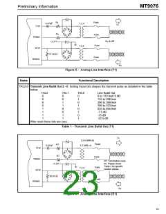
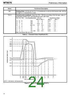
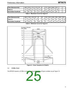
23

 MITEL [ MITEL NETWORKS CORPORATION ]