MT9041B
Advance Information
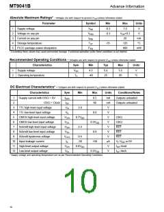
Absolute Maximum Ratings* - Voltages are with respect to ground (V ) unless otherwise stated.
SS
Parameter
Symbol
Min
Max
Units
1
2
3
4
5
Supply voltage
VDD
-0.3
-0.3
7.0
VDD+0.3
20
V
V
Voltage on any pin
Current on any pin
Storage temperature
V
PIN
PIN
I
mA
°C
TST
-55
125
PLCC package power dissipation
P
900
mW
PD
* Exceeding these values may cause permanent damage. Functional operation under these conditions is not implied.
Recommended Operating Conditions - Voltages are with respect to ground (VSS) unless otherwise stated.
Characteristics
Supply voltage
Operating temperature
Sym
Min
Typ
Max
Units
1
2
VDD
TA
4.5
-40
5.0
25
5.5
85
V
°C
DC Electrical Characteristics* - Voltages are with respect to ground (VSS) unless otherwise stated.
Characteristics
Sym
Min
Max
Units
Conditions/Notes
1
2
3
4
5
6
7
8
9
Supply current with:OSCi = 0V
IDDS
IDD
0.5
60
mA
mA
V
Outputs unloaded
Outputs unloaded
OSCi = Clock
TTL high-level input voltage
TTL low-level input voltage
CMOS high-level input voltage
CMOS low-level input voltage
Schmitt high-level input voltage
Schmitt low-level input voltage
Schmitt hysteresis voltage
VIH
2.0
VIL
0.8
V
VCIH
VCIL
VSIH
VSIL
VHYS
IIL
0.7V
V
OSCi
OSCi
RST
RST
RST
DD
0.3V
V
DD
2.3
V
0.8
V
0.4
-50
V
10 Input leakage current
11 High-level output voltage
12 Low-level output voltage
+50
uA
V
V =V or 0V
I DD
VOH
VOL
0.8V
IOH=4mA
IOL=4mA
DD
0.2V
V
DD
* Supply voltage and operating temperature are as per Recommended Operating Conditions.
10

 MITEL [ MITEL NETWORKS CORPORATION ]