MT8986
Interface
Clock
required at
CLK Pin
(MHz)
Variable/
Constant
throughput
Delay
Number of
Input x
Serial
Interface
Data Rate
Matrix
Channel
Capacity
Input/Output
Streams Used
Output
Streams
Selection
2 Mb/s
4.096
4.096
8x8
256x256 Non-Blocking
512x256 Blocking
STi0-7/STo0-7
STi0-15/STo0-7
Yes
No
2 Mb/s
*
16x8
*
2 Mb/s
*
4.096
4.096
10x10
*
128x128 Non-Blocking
(only 4 input x 4-output
can be selected)
STi0-9/STo0-9
STi0-7/STo0-3
Yes
No
Nibble
Switching
(2 Mb/s)
8x4
512x256 Nibbles
4 Mb/s
4 Mb/s
8 Mb/s
4.096
4.096
8.192
8x4
4x4
2x2
512x256 Blocking
256x256 Non-Blocking
256x256 Non-Blocking
STi0-7/STo0-3
STi0-3/STo0-3
STi0-1/STo0-1
No
Yes
Yes
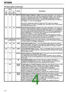
Table 1. Switching Configurations for Identical Input and Output Data Rates
* - only in the 44 pin packages
Input Frame Offset Selection
Different Input/Output Data Rates
When 4.096 or 8.192 Mb/s serial interfaces are
selected, the MT8986 device provides a feature
called Input Frame Offset allowing the user to
compensate for the varying delays at the incoming
serial inputs while building large switch matrices.
Usually, different delays occur on the digital
When Different I/O rate is selected by the DMO bit,
the input and output data rates should be selected at
the IDR and ODR bits, respectively. The Switching
Configuration Bits (SCB) are ignored with this
operation. This selection allows the user to multiplex
conventional 2.048 Mb/s serial streams into two
higher rates and vice-versa. In addition to the rate
conversion itself, the MT8986 allows for a complete
256 x 256 channel non-blocking switch at different
rates. In this operation, the per-channel variable/
constant throughput delay selection is provided.
backplanes
causing
the
data
and
frame
synchronization signals to be skewed at the input of
the switch device. This may result in the system
frame synchronization pulse to be active at the
MT8986 FR input before the first bit of the frame is
received at the serial inputs.
When the input frame offset is enabled, an "internal
delay" of up to four clock periods is added to the
actual data input sampling, providing the MT8986
serial timing unit a new input frame reference. An
internal virtual frame is created which is aligned with
the framing of the actual serial data coming in at the
serial inputs and not with the FR frame pulse input.
In this operation, the transmission of the output
frame on the serial links is still aligned to the frame
pulse input signal (FR).
Depending on which data rates are programmed for
input and output streams, the number of data
streams used on the input and output as well as the
serial interface clock (CLK input pin) is different.
Once the CPU defines the data rates at the IDR and
ODR bits, the MT8986 automatically configures itself
with the appropriate number of input and output
streams for the desired operation. Table
2
summarizes the four options available when MT8986
is used with different I/O rates. Figures 22 to 25
show the timing for each of the four modes shown in
Table 2.
The selection of the data input sampling delay is
defined by the CPU in the Frame Input Offset
Interface
Number
Variable/
Constant
throughput
Delay
Selection
Input and
Output
Data Rates
Clock
required at
CLK Pin
(MHz)
of Input
x Output
Streams
Matrix
Channel Capacity
Input/Output
Streams Used
2 Mb/s to 4 Mb/s
2 Mb/s to 8 Mb/s
4 Mb/s to 2 Mb/s
8 Mb/s to 2 Mb/s
4.096
8.192
4.096
8.192
8x4
8x2
4x8
2x8
256x256 Non-Blocking
256x256 Non-Blocking
256x256 Non-Blocking
256x256 Non-Blocking
STi0-7/STo0-3
STi0-7/STo0-1
STi0-3/STo0-7
STi0-1/STo0-7
Yes
Yes
Yes
Yes
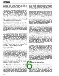
Table 2. Switching Configurations for Different I/O Data Rates
2-70

 MITEL [ MITEL NETWORKS CORPORATION ]