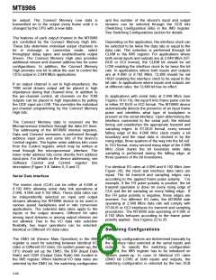
MT8986
Data Rate
Throughput Delay (d)
2.048 Mb/s
4.096 Mb/s
8.192 Mb/s
d=[32 + (32 - IN) + (OUT - 1)]; (expressed in # time-slots)
2.048 Mb/s time-slot: 3.9µs
IN: input time-slot (from 1 to 32)
OUT: output time-slot (from 1 to 32)
d=[64 + (64 - IN) + (OUT - 1)]; (expressed in # time-slots)
4.096 Mb/s time-slot: 1.95 µs
IN: input time-slot (from 1 to 64)
OUT: output time-slot (from 1 to 64)
d=[128 + (128 - IN) + (OUT - 1)]; (expressed in # time-slots)
8.192 Mb/s time-slot: 0.975 µs
IN: input time-slot (from 1 to 128)
OUT: output time-slot (from 1 to 128)
Table 4. Constant Throughput Delay values
operations by making use of a multiple Data-Memory
buffer technique. The input channels written in any of
the buffers during frame N will be read out during
frame N+2. In applications at 2.048 Mb/s for
instance, the minimum throughput delay achievable
in constant delay mode will be 32 time-slots; for
example, when input time-slot 32 (channel 31) is
switched to output time-slot 1 (channel 0). Likewise,
the maximum delay is achieved when the first time
slot in a frame (channel 0) is switched to the last
time-slot in the frame (channel 31), resulting in 94
time-slots of delay.
the level of the DS/RD input pin at the rising edge of
the AS/ALE to identify the appropriate bus timing
connected to the MT8986. If DS/RD is LOW at the
rising edge of AS/ALE then Motorola bus timing is
selected. If DS/RD is HIGH at the rising edge of AS/
ALE, then Intel bus timing is selected.
When MT8986 parallel port is operating in Motorola,
National or Intel multiplexed bus interfaces, the
signals available for controlling the device are: AD0-
AD7 (Data and Address), ALE/AS (Address Latch
Enable/Address Strobe), DS/RD (Data Strobe/
Read), R/W\WR (Read/Write\Write), CS (Chip
Select) and DTA (Data Acknowledgement). In
Motorola non-multiplexed bus, the interface control
signals are: data bus (AD0-AD7), six address input
lines (A0-A5) and four control lines (CS , DS, R/W
and DTA). See Figures 26 to 28 for each CPU
interface timing.
To summarize, any input time-slot from input frame N
will always be switched to the destination time-slot
on output frame N+2. Table 4 describes the MT8986
constant throughput delay values for different data
rates.
Microprocessor Port
The MT8986 parallel microport provides the access
to the IMS, Control registers, the Connection
Memory High, the Connection Memory Low and the
Data Memory. All locations can be read or written
except for the data memory which can be read only.
The non-multiplexed bus interface provided by the
MT8986 device is identical to that provided in
MT8980 Digital Switch device. In addition to the non-
multiplexed bus, the MT8986 device provides an
enhanced microprocessor interface with multiplexed
bus structure compatible to both Motorola and Intel
buses. The multiplexed bus structure is available
only in the 44 pin packages and it is selected by the
CPU Interface Mode (IM) input pin.
Software Control
The address bus on the microprocessor interface
selects the internal registers and memories of the
MT8986. If the A5 address input is LOW, then the
MT8986 Internal Control, Interface Mode, Stream
Pair Selection and Frame Input Offset registers are
addressed by the A4 to A0 bits according to Table 5.
If A5 input is HIGH, then the remaining address input
lines are used to select memory subsections of up to
128 locations corresponding to the maximum
number of channels per input or output stream. The
address input lines and the Stream Address bits
(STA) of the Control register give the user the
capability of accessing all sections of the MT8986
Data and Connect memories.
If IM input pin is not connected (left open) or
grounded, the MT8986 parallel port assumes its
default Motorola non-multiplexed bus mode identical
to that of MT8980. If IM input is connected HIGH, the
internal parallel microport provides compatibility to
MOTEL interface allowing direct connection to Intel,
National and Motorola CPUs.
The MOTEL circuit (MOtorola and InTEL compatible
bus) automatically identifies the type of CPU Bus
connected to the MT8986 device. This circuit uses
2-72

 MITEL [ MITEL NETWORKS CORPORATION ]