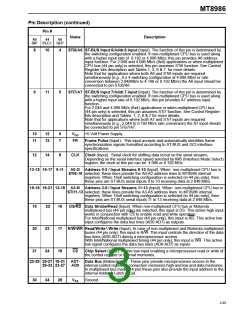
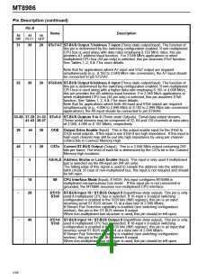
MT8986
be output. The Connect Memory Low data is
transmitted on to the output every frame until it is
changed by the CPU with a new data.
and the number of the device's input and output
streams can be selected through the SCB bits
(Switching Configuration Bits) in the IMS register.
See Switching Configurations section for details.
The features of each output channel in the MT8986
are controlled by the Connect Memory High bits.
These bits determine individual output channels to
be in message or connection mode, select
throughput delay types and enable/disable output
drivers. The Connect Memory High also provides
additional stream and channel address bits for some
configurations. In addition, the Connect Memory
High provides one bit to allow the user to control the
CSTo output in 2.048 Mb/s applications.
Depending on the application, the interface clock can
be selected to be twice the data rate or equal to the
data rate. This selection is performed through bit
CLKM in the IMS register. For applications where
both serial inputs and outputs are at 2.048 Mb/s (ST-
BUS or GCI format), the CLKM bit should be set
LOW enabling the interface clock to be twice the bit
rate. In applications where both inputs and outputs
are at 4.096 or 8.192 Mb/s, CLKM should be set
HIGH enabling the interface clock to be equal to the
bit rate. In applications where inputs and outputs are
at different rates, the CLKM bit has no effect.
If an output channel is set to high-impedance, the
TDM serial stream output will be placed in high
impedance during that channel time. In addition to
the per-channel control, all channels on the TDM
outputs can be placed in high impedance by pulling
the ODE input pin LOW. This overrides the individual
per-channel programming by the Connect Memory
High bits.
In applications with serial links at 2.048 Mb/s (see
Figures 16 to 19), the input 8 kHz frame pulse can be
in either ST-BUS or GCI format. The MT8986 device
automatically detects the presence of an input frame
pulse and identifies what type of backplane is
present on the serial interface. Upon determining the
interface connected to the serial port, the internal
timing unit establishes the appropriate transmit and
sampling edges. In ST-BUS format, every second
falling edge of the 4.096 MHz clock marks a bit
boundary and the input data is clocked in by the
rising edge, three quarters of the way into the bit cell.
In GCI format, every second rising edge of the 4.096
MHz clock marks the bit boundary while data
sampling is performed during the falling edge, at
three quarters of the bit boundaries.
The Connect Memory data is received via the
Microprocessor Interface through the data I/O lines.
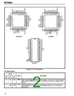
The addressing of the MT8986 internal registers,
Data and Connect memories is performed through
address input pins and some bits of the device's
Control register. The higher order address bits come
from the Control register, which may be written or
read through the microprocessor interface. The
lower order address bits come directly from address
input pins. For details on the device addressing, see
Software Control and Control register bits
description (Figure 3 & Tables 5, 6 and 7).
For identical I/O rates at 4.096 and 8.192 Mb/s (see
Figure 20), the clock and interface data rates are
equal. The bit transmit and sampling edges vary
according to the applied frame pulse polarity. For
example, if the FR pulse polarity is positive, the bit
transmit operation is done on every rising edge of
CLK and the bit sampling on every falling edge. If
the FR pulse polarity is negative, these edges are
inverted. For different I/O rates, the MT8986 side
operating at 2.048 Mb/s data rate will comply with
ST-BUS or GCI interfaces for transmit and sampling
procedures. The MT8986 side operating at 4.096 or
8.192 Mb/s behaves according to the frame pulse
polarity applied. See Figures 22 to 25.
Serial Data Interface
The master clock (CLK) can be either at 4.096 or
8.192 MHz allowing serial data link operations at
2.048, 4.096 and 8.192 Mb/s. These data rates can
be independently selected on input and output
streams allowing the MT8986 device to be used in
various speed backplanes and in rate conversion
applications. The selected data rates apply to the
inputs or the output streams. Different bit rates
among input streams or among output streams are
not allowed. Due to the I/O data rate selection
flexibility, two major operations can be selected:
Identical or Different I/O data rates.
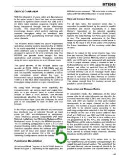
Switching Configurations
The DMO bit (Device Main Operation) in the IMS
register is used for selecting between Identical I/O
rates or Different I/O rates. On system power-up, the
CPU should set up the DMO, the IDR (Input Data
Rate) and ODR (Output Data Rate) bits located in
the IMS register. When Identical I/O data rates are
selected by the DMO bit, the switching configuration
Switching configurations are determined basically by
the interface rates selected at the serial inputs and
outputs. To specify the switching configuration
required, the IMS register has to be initialized on
system power-up. In case of Identical I/O rates
(DMO bit LOW) at both inputs and outputs, the
switching configuration is selected by the two SCB
2-68

 MITEL [ MITEL NETWORKS CORPORATION ]