MT8986
MT8986 device receives TDM serial data at different
rates and from different number of serial streams.
DEVICE OVERVIEW
With the integration of voice, video and data services
in the same network, there has been an increasing
demand for systems which ensure that data at N x
64 kbit/s rates maintain sequence integrity while
being transported through time-slot interchange
circuits. This requirement demands time-slot
interchange devices which perform switching with
constant throughput delay for wideband data
applications while guaranteeing minimum delay for
voice channels.
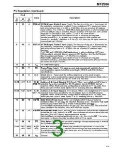
Data and Connect Memories
For all data rates, the received serial data is
converted to parallel format by the serial to parallel
converters and stored sequentially in
a Data
Memory. Depending on the selected operation
programmed in the IMS (Interface Mode Select)
register, the Data Memory may have up to 512 bytes
in use. The sequential addressing of the Data
Memory is performed by an internal counter which is
reset by the input 8 kHz frame pulse (FR) marking
the frame boundaries of the incoming serial data
streams.
The MT8986 device meets the above requirement
and allows existing systems based on the MT8980D
to be easily upgraded to maintain the data integrity
when wideband data is transported. The device is
designed to switch 32, 64 or N x 64 kbit/s data. The
MT8986 can provide frame integrity for data
applications and minimum throughput switching
delay for voice applications on a per channel basis.
Data to be output on the serial streams may come
from two sources: Data Memory or Connect Memory.
Locations in the Connect Memory, which is split into
HIGH and LOW parts, are associated with particular
ST-BUS output streams. When a channel is due to
be transmitted on an ST-BUS output, the data for the
channel can either be switched from an ST-BUS
input as in connection mode or it can be from the
Connect Memory Low as in message mode. Data
destined for a particular channel on the serial output
stream is read from the Data Memory or Connect
Memory Low during the previous channel time-slot.
This allows enough time for memory access and
parallel to serial conversion.
The serial streams of the MT8986 device can
operate at 2.048, 4.096 or 8.192 Mbit/s and are
arranged in 125 µs wide frames which contain 32, 64
and 128 channels, respectively. In addition, a built-in
rate conversion circuit allows the user to
interconnect various backplane speeds like 2.048 or
4.096 or 8.192 Mb/s while maintaining the control of
throughput delay function on a per-channel basis.
By using Mitel Message mode capability, the
microprocessor can access input and output time-
slots on a per channel basis to control external
circuits or other ST-BUS devices. The MT8986
automatically identifies the polarity of the frame
synchronization input signal and configures its serial
port to be compatible to both ST-BUS and GCI
formats.
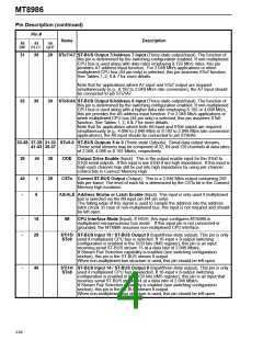
Connection and Message Modes
In connection mode, the addresses of the input
source data for all output channels are stored in the
Connect memories High (CMH) and Low (CML). The
CML and CMH are mapped so that each location
corresponds to an output channel on the output
streams. The number of source address bits in CMH
and CML to be utilized varies according to the
switching configuration selected in the IMS register.
For details on the use of the source address data
(CAB and SAB bits), see CMH and CML bit descrip-
tion (Figures 5 & 6). Once the source address bits
are programmed by the CPU, the contents of the
Data Memory at the selected address are transferred
to the parallel-to-serial converters. By having the
output channel specify the source channel through
the connect memory, the user can route the same
input channel to several output channels, allowing
broadcast facility within the switch.
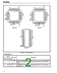
In the 44 pin packages, two different microprocessor
bus interfaces can be selected through an input
mode pin (IM): Non-Multiplexed or Multiplexed.
These interfaces provide compatibility with Intel/
National multiplexed and Motorola Multiplexed/Non-
Multiplexed buses. In 44 pin, the MT8986 provides a
16 x 8 switching configuration to form a 512 x 256
channel blocking matrix. Also, a flexible Stream Pair
Selection operation allows the software selection of
which pair of input and output streams can be
connected to an internal 128 x 128 matrix. See
Switching Configurations section for details.
In message mode the CPU writes data to the
Connect Memory Low locations corresponding to the
output link and channel number. The contents of the
Connect Memory Low are transferred directly to the
parallel-to-serial converter one channel before it is to
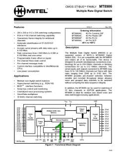
Functional Description
A functional Block Diagram of the MT8986 device is
shown in Figure 1. Depending on the application, the
2-67

 MITEL [ MITEL NETWORKS CORPORATION ]