MT8931C
AC Electrical Characteristics† - Intel Bus Interface Timing (Ref. Figure 24 & 25)
‡
Characteristics
Sym
Min
Typ
Max
Units
Test Conditions
1
2
Chip select setup time
Chip select hold time
Address Latch pulse width
Address setup time
Address hold time
tCSS
tCSH
tALW
tADS
tADH
tDWS
tDHW
tDOD
tDHR
tWPW
tRWD
tRPW
tRDS
10
25
50
20
20
35
20
ns
ns
ns
ns
ns
ns
ns
ns
ns
ns
ns
ns
ns
3
4
5
6
Data setup time - Write
Data hold time - Write
Data output delay - Read
Data hold time - Read
Write pulse width
7
8
240
90
50 pF load
50 pF load
9
25
60
10
11
12
13
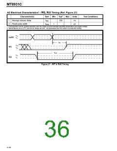
RD, WR delay
60
Read pulse width
240
Read setup time
20
† Timing is over recommended temperature & power supply voltages
‡ Typical figures are at 25°C and are for design aid only: not guaranteed and not subject to production testing.
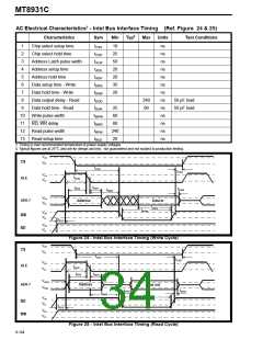
VIH
CS
VIL
tCSS
tCSH
VIH
VIL
tALW
tADS
ALE
tADH
tDHW
tRWD
VIH
VIL
AD0-7
Address
Data in
tDWS
tWPW
VIH
VIL
WR
RD
tRDS
VIH
VIL
Figure 24 - Intel Bus Interface Timing (Write Cycle)
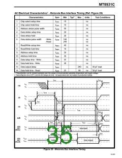
VIH
VIL
CS
tCSS
tCSH
VIH
VIL
ALE
tALW
tADS
tADH
VI/OH
VI/OL
AD0-7
Address
Data out
tRPW
tDOD
tDHR
tRWD
VIH
VIL
RD
tRDS
VIH
VIL
WR
Figure 25 - Intel Bus Interface Timing (Read Cycle)
9-104

 MITEL [ MITEL NETWORKS CORPORATION ]