MT8931C
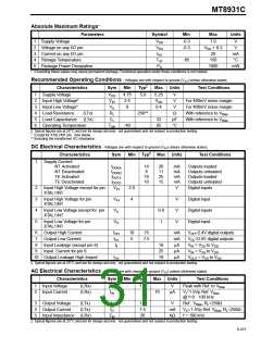
Absolute Maximum Ratings*
Parameters
Symbol
Min
Max
Units
1
2
3
4
5
Supply Voltage
VDD
VI/O
II/O
-0.3
-0.3
7.0
VDD + 0.3
20
V
V
Voltage on any I/O pin
Current on any I/O pin
Storage Temperature
Package Power Dissipation
mA
°C
TST
PD
-65
150
1000
mW
* Exceeding these values may cause permanent damage. Functional operation under these conditions is not implied.
Recommended Operating Conditions - Voltages are with respect to ground (VSS) unless otherwise stated.
‡
Characteristics
Supply Voltage
Sym
Min
Typ
Max
Units
Test Conditions
1
2
3
4
5
6
VDD
VIH
VIL
RL
4.75
2.4
0
5.0
5.25
VDD
0.4
V
V
Input High Voltage*
Input Low Voltage*
Load Resistance
Load Capacitance
For 400mV noise margin
For 400mV noise margin
With reference to VBias
With reference to VBias
V
(LTx)
(LTx)
250**
Ω
CL
32
85
pF
°C
Operating Temperature
TOP
-40
‡ Typical figures are at 25°C and are for design aid only: not guaranteed and not subject to production testing.
* Except for XTAL1/NT pin. See below.
** Including the transformer DC resistance.
DC Electrical Characteristics - Voltages are with respect to ground (VSS) unless otherwise stated.
‡
Characteristics
Sym
Min Typ
Max Units
Test Conditions
1
Supply Current
NT Activated
NT Deactivated
TE Activated
IDDNA
IDDND
IDDTA
IDDTD
14
8
16
10
20
11
25
15
mA
mA
mA
mA
Outputs loaded
Outputs unloaded
Outputs loaded
TE Deactivated
Outputs unloaded
2
3
4
5
Input High Voltage except for pin
XTAL1/NT
VIH
VIH
VIL
VIL
2.0
4
V
V
V
V
Digital inputs
Digital input
Digital inputs
Digital input
Input High Voltage for pin
XTAL1/NT
Input Low Voltage except for pin
XTAL1/NT
0.8
1
Input Low Voltage for pin
XTAL1/NT
6
7
8
9
Output High Current
IOH
IOL
IiI
10
5
15
mA
mA
µA
µA
µA
VOH=2.4V digital outputs
VOL=0.4V digital outputs
VIN = VSS to VDD
Output Low Current
7.5
Input Leakage (except pin 8)
Input Current for pin 8
10
25
10
VIN = VSS to VDD
10 Output Leakage High Imped.
IOZ
VOUT = VSS to VDD
‡ Typical figures are at 25°C and are for design aid only: not guaranteed and not subject to production testing.
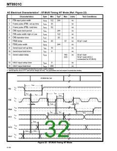
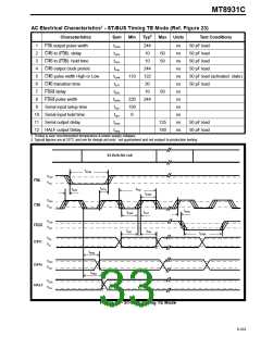
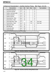
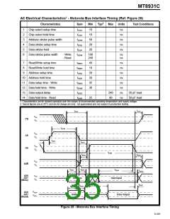
AC Electrical Characteristics - Voltages are with respect to ground (VSS) unless otherwise stated.
‡
Characteristics
Sym
Min
Typ
Max Units
Test Conditions
1
2
Input Voltage
(LRx)
(LRx)
VIN
IIN
1.5
V
Peak with Ref. to VBias
Input Current
70
µA
VI=1.5Vp Ref. VBias
@ f=0 - 100 kHz
3
4
5
Output Voltage
Output Current
(LTx)
(LTx)
VO
IO
1.5
7.5
20
V
Ref. VBias, RL=250Ω
VO=1.5Vp Ref. VBias, RL=250Ω
f = 100 kHz
mA
kΩ
Input Impedance (LRx)
ZIN
‡ Typical figures are at 25°C and are for design aid only: not guaranteed and not subject to production testing.
9-101

 MITEL [ MITEL NETWORKS CORPORATION ]