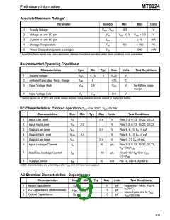
MT8924
Preliminary Information
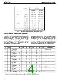
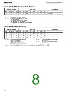
PCM Byte
+ve input -ve input
Noise
Threshold
B7 - B0
B7 - B0
A-Law
1/4096
9/4096
1000 0000
1000 0100
1000 1000
1000 1111
1111 1111
1111 1011
1111 0111
1111 0000
0000 0000
0000 0100
0000 1000
0000 1111
0111 1111
0111 1011
0111 0111
0111 0000
16/4096
32/4096
1/8159
µ-Law
9/8159
16/8159
32/8159
Table 1 - PCM Noise Suppression Threshold Levels
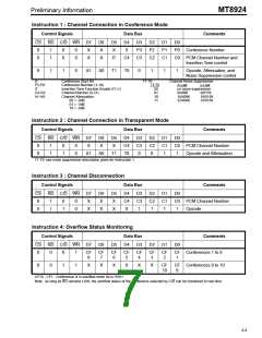
Overflow Detection / Input Channel Attenuation
If the sum of the channels involved in one conference
exceeds the full scale value of the accumulator, an
overflow condition is generated which can be
monitored specifically by reading the status of the
overflow register. If an overflow condition occurs,
Alternatively, a conference in the overflow condition
can be detected using the OS signal in conjunction
with frame pulse F0i. OS will be low during the
second half of a general output channel slot time N,
if channel N belongs to a conference in overflow (see
Figure 11). This information can be used to control
input channel attenuation through software control.
then each channel in
a
conference can be
independently attenuated if desired.
F1
F0
B7
B6
B5
B4
B3
B2
B1
B0
Comments
No Inversion
0
0
+ Full Scale
+ 0 Level
1
1
0
0
1
1
0
0
1
1
0
0
1
1
0
0
1
0
0
1
0
1
1
0
1
0
0
1
0
1
1
0
1
0
0
1
1
0
0
1
0
1
1
0
0
1
1
0
1
0
0
1
0
1
1
0
1
0
0
1
0
1
1
0
1
0
0
1
1
0
0
1
0
1
1
0
0
1
1
0
1
0
0
1
0
1
1
0
1
0
0
1
0
1
1
0
1
0
0
1
1
0
0
1
0
1
1
0
0
1
1
0
1
0
0
1
0
1
1
0
1
0
0
1
0
1
1
0
- 0 Level
- Full Scale
+ Full Scale
+ 0 Level
0
1
1
1
0
1
Even Bit Inversion
Odd Bit Inversion
Bit Inversion
- 0 Level
- Full Scale
+ Full Scale
+ 0 Level
- 0 Level
- Full Scale
+ Full Scale
+ 0 Level
- 0 Level
- Full Scale
Table 2 - PCM Byte Format
B7 (sign bit) is the MSB and B0 is the LSB
F1-F0 corresponds to the D5-D4 bits of the control byte of Operating Mode Instruction 5
8-6

 MITEL [ MITEL NETWORKS CORPORATION ]