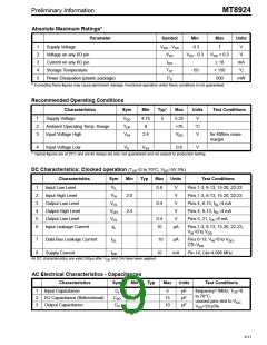
MT8924
Preliminary Information
24
23
22
21
20
19
18
17
16
15
14
13
1
2
3
4
5
6
7
8
TD
TF
RESET
OS
DSTo
VSS
A/µ
DSTi
Cko
Cki
F0i
WR
RD
D7
D6
D5
D4
D3
D2
D1
CS
9
C/D
VDD
D0
10
11
12
Figure 2 - Pin Connections
Pin Description
Pin #
Name
Description
1
TD
Tone Duration (Input). When TD is High, a PCM-coded tone is sent out to all channels of
the enabled conferences instead of PCM data. TD is latched by frame pulse F0i so that all
channels have the same tone during the same frame number. When TD is Low, normal
operation is enabled.
2
3
TF
Tone Frequency (Input). This input is connected to an external squarewave generator. TF
is strobed by frame pulse F0i so that all channels have the same tone frequency during the
same number of frames. The PCM-coded tone level corresponds to 1/10th of the full scale
value, and is activated when TD is High.
RESET Master RESET (Input). This input is used for system reset after power up, or when the
companding law format has been changed. The RESET pin is strobed by the rising edge of
clock Cki. Complete circuit initialization takes two frame periods. Resetting the device
disables the output drivers of the microprocessor interface and DSTo.
4
5
OS
Overflow Signalling (Output). When OS is Low, a conference is in the overflow condition.
This signal is delayed by half of a timeslot relative to the beginning of the output channel of
the conference in overflow (see Figure 9).
DSTo
ST-BUS Serial Output. This pin is the output for the PCM signal. It is enabled upon
channel selection, otherwise it is placed in a high impedance state. Maximum bit rate is
2.048 Mb/s.
6-13 D7 to D0 Data Bus I/O Port. These are bidirectional data pins over which data and instructions are
transferred to and from the microprocessor (where D0 is the least significant bit). The bus is
in a high impedance state when RESET is Low and/or CS is High.
14
15
VDD
C/D
Positive Supply Voltage. Nominally 5 volts.
Control/Data Select (Input). The signal on this input defines whether the information on the
data bus should be interpreted as opcode or data. During a write operation a Low signal
defines the bus content as data, while a High signal defines it as opcode. During a read
operation this input differentiates overflow status between the first eight channels for C/D
being LOW, and the last two channels for C/D being HIGH (see Instruction 4). This input also
allows status monitoring (see Instruction 6) during a read operation.
16
CS
Chip Select (Input). This active low input selects the device for microprocessor read/write
operations. When CS is Low, data and instructions can be transferred to or from the
microprocessor, and when CS is High, the data bus is in a high impedance state.
17
18
RD
Read (Input). This active low input is for the read signal on the microprocessor interface.
The data bus is updated on the falling edge of RD.
WR
Write Input. This active low input is for the write signal on the microprocessor interface. The
data bus is strobed on the rising edge of WR.
8-4

 MITEL [ MITEL NETWORKS CORPORATION ]