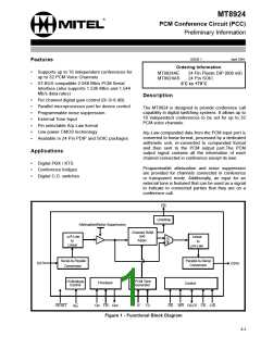
Preliminary Information
MT8924
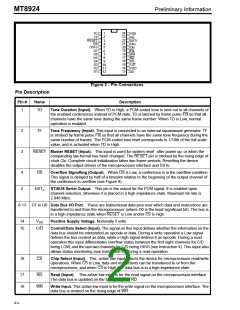
Pin Description (continued)
Pin #
Name
Description
19
F0i
Frame Pulse (Input). This is an 8 kHz active low input used for frame synchronization of the
PCM bit stream. The first falling edge of Cki following the falling edge of frame pulse F0i
determines the start of a new frame and must correspond to the first bit of the first channel.
When PCM frames of 1544 kbit/s are used, the rising edge of F0i must correspond to the
Extra (193rd) bit.
20
21
Cki
Clock (Input). This signal is the timing reference used for all internal operations. The PCM
bit cell boundaries lie on the alternate falling edges of this clock. The maximum allowable
clock frequency is 4096 kHz.
Cko
Clock (Output). This pin provides the master clock for a digital crosspoint switch (e.g.,
MT898x series, or the MT9080, MT9085 combination). Normally the signal on this pin is
identical to Cki. When Extra bit operating mode is selected (see Instruction 5), the first two
cycles of the master clock are suppressed (see Figure 10). This feature allows the MT8924
to operate in 1544 kbit/s systems.
22
DSTi
ST-BUS Serial Input. This pin accepts the serial PCM input stream at a maximum allowable
bit rate of 2048 kbit/s. In normal operation the first bit of the first channel is defined by the
rising edge of Cki following the falling edge of frame pulse F0i. When Extra bit operating
mode is selected, the first bit of the first channel defines the extra bit.
23
24
A/µ
A/µ - Law Select Input. When A/µ is High, A-Law is selected, and when A/µ is Low, µ-Law is
selected. The companding law selection must be done before initializing the device using the
RESET pin.
VSS
Negative Power Supply Voltage. Nominally 0 Volts.
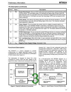
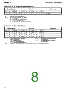
channel N+1, frame M and subtracted during the
Functional Description
second half of channel N-1, frame M+1. After Linear-
to-PCM conversion the subtraction result goes to the
parallel-to-serial converter, and appears at the
output on the N+1 channel, M+1 frame with respect
to the corresponding sending party information (see
Figure 4).
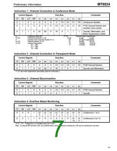
The MT8924 is a device designed to provide
conferencing in a digital switching system in any
combination for up to all 32 channels of a 2048 kbit/s
ST-BUS stream (see Figure 3).
The information of channel N, frame M is first
converted to Linear PCM and then added to the
signal from other conferencees during the first half of
To a microprocessor the MT8924 appears as a
memory mapped peripheral device that can be
controlled by a set of six instructions. These
commands can be used to establish or cancel
conferences between the PCM channels and also to
transmit control messages on specific operating
modes. The microprocessor can initiate and receive
status messages or check conference connections
that are currently in operation.
Microcontroller
STi0
.
.
.
.
STo0
.
.
.
.
MT8980/81/82
Digital Switch
Output
Input
STix-1
STox-1
Information
Information
B+C A+C A+B
B
C
A
STix
STox
DSTo
DSTi
MT8924
N+1 N+2 N+3
N
N+1 N+2
MT8924
PCM Conference
Circuit (PCC)
Output Channels
Frame M+1
Input Channels
Frame M
Figure 4 - Input/Output Channel Relationship
Figure 3 -Typical Conference Connection
8-5

 MITEL [ MITEL NETWORKS CORPORATION ]