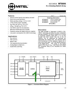
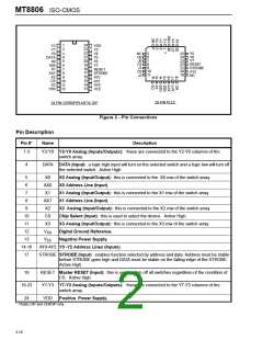
ISO-CMOS MT8806
AC Electrical Characteristics† - Crosspoint Performance - Voltages are with respect to VDD=5V, VSS=0V,
VEE=-7V, unless otherwise stated.
‡
Characteristics
Sym
Min
Typ
Max Units
Test Conditions
f=1 MHz
f=1 MHz
1
2
3
Switch I/O Capacitance
Feedthrough Capacitance
C
C
20
0.2
45
pF
pF
S
F
Frequency Response
Channel “ON”
F
MHz Switch is “ON”; V
= 2Vpp
INA
3dB
sinewave; R = 1kΩ
L
20LOG(V
/V )=-3dB
See Appendix, Fig. A.3
OUT Xi
4
5
Total Harmonic Distortion
(See G.5, G.6 in Appendix)
THD
FDT
0.01
-95
%
Switch is “ON”; V = 2Vpp
INA
sinewave f= 1kHz; R =1kΩ
L
Feedthrough
dB
All Switches “OFF”; V
=
INA
Channel “OFF”
2Vpp sinewave; f= 1kHz;
Feed.=20LOG (V
/V )
R = 1kΩ.
OUT Xi
L
(See G.8 in Appendix)
See Appendix, Fig. A.4
6
Crosstalk between any two
channels for switches Xi-Yi and
Xj-Yj.
X
-45
-90
-85
-80
dB
dB
dB
dB
V
=2Vpp sinewave
INA
talk
f= 10MHz; R = 75Ω.
L
V
=2Vpp sinewave
INA
f= 10kHz; R = 600Ω.
L
Xtalk=20LOG (V /V ).
Yj Xi
V
=2Vpp sinewave
INA
f= 10kHz; R = 1kΩ.
L
(See G.7 in Appendix).
V
=2Vpp sinewave
INA
f= 1kHz; R = 10kΩ.
L
Refer to Appendix, Fig. A.5
for test circuit.
7
Propagation delay through
switch
t
30
ns
R =1kΩ; C =50pF
L L
PS
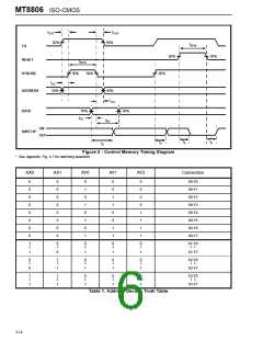
† Timing is over recommended temperature range. See Fig. 3 for control and I/O timing details.
‡ Typical figures are at 25°C and are for design aid only; not guaranteed and not subject to production testing.
Crosstalk measurements are for Plastic DIPS only, crosstalk values for PLCC packages are approximately 5dB better.
AC Electrical Characteristics† - Control and I/O Timings- Voltages are with respect to VDD=5V, VSS=0V,
V
EE=-7V, unless otherwise stated.
‡
Characteristics
Control Input crosstalk to switch
Sym
Min
Typ
Max
Units
Test Conditions
V =3V squarewave;
1
CX
30
mVpp
talk
IN
(for CS, DATA, STROBE, Address)
R =1kΩ, R =10kΩ.
IN L
See Appendix, Fig. A.6
f=1MHz
2
3
4
5
6
7
8
9
Digital Input Capacitance
C
F
10
pF
MHz
ns
DI
Switching Frequency
20
O
Setup Time DATA to STROBE
Hold Time DATA to STROBE
Setup Time Address to STROBE
Hold Time Address to STROBE
Setup Time CS to STROBE
Hold Time CS to STROBE
t
10
10
10
10
10
10
20
40
R = 1kΩ, C =50pF
L L
DS
t
ns
R = 1kΩ, C =50pF
L L
DH
t
t
ns
R = 1kΩ, C =50pF
L L
AS
AH
ns
R = 1kΩ, C =50pF
L L
t
t
ns
R = 1kΩ, C =50pF
L L
CSS
CSH
SPW
RPW
ns
R = 1kΩ, C =50pF
L L
10 STROBE Pulse Width
t
ns
R = 1kΩ, C =50pF
L L
11 RESET Pulse Width
t
ns
R = 1kΩ, C =50pF
L L
12 STROBE to Switch Status Delay
13 DATA to Switch Status Delay
14 RESET to Switch Status Delay
t
t
t
40
50
35
100
100
100
ns
R = 1kΩ, C =50pF
L L
S
D
R
ns
R = 1kΩ, C =50pF
L L
ns
R = 1kΩ, C =50pF
L L
† Timing is over recommended temperature range. See Fig. 3 for control and I/O timing details.
Digital Input rise time (tr) and fall time (tf) = 5ns.
‡ Typical figures are at 25°C and are for design aid only; not guaranteed and not subject to production testing.
Refer to Appendix, Fig. A.7 for test circuit.
3-13

 MITEL [ MITEL NETWORKS CORPORATION ]