MT8806 ISO-CMOS
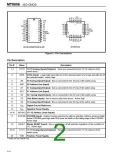
24
23
22
21
20
19
18
17
16
15
14
13
1
2
3
4
5
6
7
8
Y2
Y1
Y0
VDD
Y3
Y4
Y5
Y6
•
Y5
NC
5
25
24
23
22
21
20
19
Y6
6
DATA
X0
AX0
X1
AX1
X2
CS
D0
Y7
J0
7
D1
J1
8
RESET
STROBE
AY2
NC
Y7
9
RESET
STROBE
AY2
AY1
AY0
VEE
10
11
D2
J2
9
10
11
12
X3
VSS
28 PIN PLCC
24 PIN CERDIP/PLASTIC DIP
Figure 2 - Pin Connections
Pin Description
Pin #*
Name
Description
1-3
Y2-Y0 Y2-Y0 Analog (Inputs/Outputs): these are connected to the Y2-Y0 columns of the
switch array.
4
DATA DATA (Input): a logic high input will turn on the selected switch and a logic low will turn off
the selected switch. Active High.
5
6
X0
AX0
X1
X0 Analog (Input/Output): this is connected to the X0 row of the switch array.
X0 Address Line (Input).
7
X1 Analog (Input/Output): this is connected to the X1 row of the switch array.
X1 Address Line (Input).
8
AX1
X2
9
X2 Analog (Input/Output): this is connected to the X2 row of the switch array.
Chip Select (Input): this is used to select the device. Active High.
X3 Analog (Input/Output): this is connected to the X3 row of the switch array.
Digital Ground Reference.
10
11
12
13
14-16
17
CS
X3
V
V
SS
EE
Negative Power Supply.
AY0-AY2 Y0 -Y2 Address Lines (Inputs).
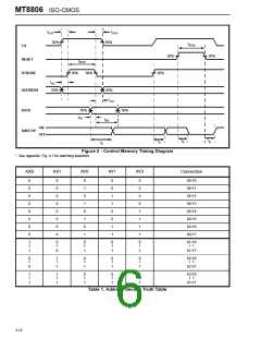
STROBE STROBE (Input): enables function selected by address and data. Address must be stable
before STROBE goes high and DATA must be stable on the falling edge of the STROBE.
Active High.
18
19-23
24
RESET Master RESET (Input): this is used to turn off all switches regardless of the condition of
CS. Active High.
Y7-Y3 Y7-Y3 Analog (Inputs/Outputs): these are connected to the Y7-Y3 columns of the
switch array.
VDD
Positive Power Supply.
* Plastic DIP and CERDIP only
3-10

 MITEL [ MITEL NETWORKS CORPORATION ]