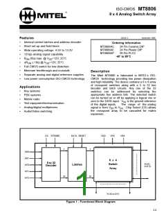
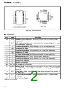
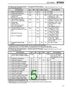
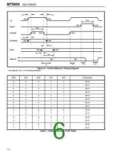
MT8806 ISO-CMOS
Absolute Maximum Ratings*- Voltages are with respect to VEE unless otherwise stated.
Parameter
Symbol
Min
Max
Units
1
Supply Voltage
V
V
-0.3
-0.3
15.0
V
V
DD
SS
V
V
V
+0.3
DD
DD
DD
2
3
4
5
6
Analog Input Voltage
Digital Input Voltage
V
-0.3
+0.3
+0.3
V
V
INA
V
V
-0.3
SS
IN
Current on any I/O Pin
Storage Temperature
I
±15
mA
°C
T
-65
+150
S
Package Power Dissipation
PLASTIC DIP
CERDIP
P
P
0.6
1.0
W
W
D
D
* Exceeding these values may cause permanent damage. Functional operation under these conditions is not implied.
Recommended Operating Conditions - Voltages are with respect to VEE unless otherwise stated.
Characteristics
Sym
Min
Typ
Max
Units
Test Conditions
1
2
Operating Temperature
Supply Voltage
T
-40
4.5
25
85
°C
O
V
V
13.2
V
V
DD
SS
V
V
-4.5
EE
DD
3
4
Analog Input Voltage
Digital Input Voltage
V
V
V
V
V
V
INA
EE
DD
DD
V
V
IN
SS
DC Electrical Characteristics†- Voltages are with respect to VEE=VSS=0V, VDD =12V unless otherwise stated.
‡
Characteristics
Sym
Min
Typ
Max
Units
Test Conditions
1
Quiescent Supply Current
I
1
100
µA
All digital inputs at V =V or
DD
IN
SS
V
DD
0.4
1.5
mA
All digital inputs at V =2.4 +
IN
V
; V =7.0V
SS
SS
5
15
mA
nA
All digital inputs at V =3.4V
IN
2
3
Off-state Leakage Current
(See G.9 in Appendix)
I
±1
±500
IV - V I = V - V
Xi Yj DD EE
OFF
See Appendix, Fig. A.1
0.8+VS
Input Logic “0” level
V
V
V
=7.5V; V =0V
EE
IL
SS
S
2.0+VSS
4
5
6
Input Logic “1” level
V
V
V
V
V
=6.5V; V =0V
EE
IH
IH
SS
Input Logic “1” level
3.3
Input Leakage (digital pins)
I
0.1
10
µA
All digital inputs at V = V
IN SS
LEAK
or V
DD
† DC Electrical Characteristics are over recommended temperature range.
‡ Typical figures are at 25°C and are for design aid only; not guaranteed and not subject to production testing.
DC Electrical Characteristics- Switch Resistance - VDC is the external DC offset applied at the analog I/O pins.
Characteristics
Sym
25°C
70°C
85°C
Units
Test Conditions
Typ Max Typ Max Typ Max
1 On-state
V
=12V
R
45
55
65
75
75
85
215
80
90
225
Ω
Ω
Ω
V
=V =0V,V =V /2,
SS EE DC DD
DD
DD
ON
Resistance V =10V
IV -V I = 0.4V
See Appendix, Fig. A.2
Xi Yj
V
= 5V
120 185
DD
(See G.1, G.2, G.3 in
Appendix)
2 Difference in on-state
resistance between two
switches
∆R
5
10
10
10
Ω
V
V
=12V, V =V =0,
SS EE
ON
DD
DC
=V /2,
DD
IV -V I = 0.4V
Xi Yj
(See G.4 in Appendix)
See Appendix, Fig. A.2
3-12

 MITEL [ MITEL NETWORKS CORPORATION ]