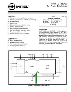
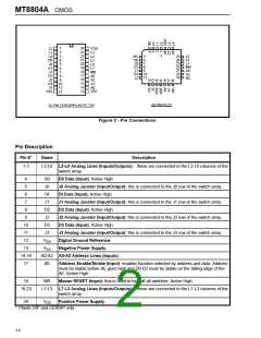
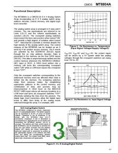
CMOS MT8804A
AC Electrical Characteristics† - Crosspoint Performance -VDC is the external DC offset applied at the analog
I/O pins. Voltages are with respect to VDD=10V, VSS=VEE=0V unless otherwise stated.
‡
Characteristics
Sym
Min
Typ
Max Units
Test Conditions
1
2
3
4
Switch Line Capacitance
Switch Junctor Capacitance
Feedthrough Capacitance
C
5
pF
pF
pF
IS
C
20
0.2
40
OS
C
I
Frequency Response
Channel “ON”
F
MHz Switch is “ON”; V =5V,
DC
3dB
V
=5Vpp sinewave
INA
20LOG(VOUT / V ) = -3dB
f= 1kHz; R = 1kΩ
INA
L
5
Total Harmonic Distortion
THD
FDT
Switch is “ON”; V
V
=0V
EE= SS
V
V
V
=15V/V =7.5V
0.1
0.2
1.0
%
%
%
V
=5Vpp sinewave
DD
DD
DD
DC
INA
=10V/V =5V
f= 1kHz;
R = 10kΩ
DC
=5V/V =2.5V
DC
L
6
7
Feedthrough
Channel “OFF”
-50
dB
All Switches “OFF”; V
INA
5Vpp sinewave f= 1MHz;
=
Feed.=20LOG (VOUT / V
)
R = 1kΩ. V =5V
INA
L
DC
Crosstalk between any two
channels for switches Li - Ji and
Lj - Jj.
X
-40
-90
dB
dB
V
=2Vpp sinewave
talk
INA
f= 1.0MHz; R = 600Ω.
L
V
=2Vpp sinewave
INA
Li - Ji is “ON“
Lj - Jj is “OFF“
f= 3.4kHz; R = 600Ω.
L
V
= 5V
DC
Xtalk=20LOG (V /V ).
Jj Li
8
Propagation delay through
switch
t
10
ns
C =50pF
L
PS
† AC Electrical Characteristics are at ambient temperature (25°C).
‡ Typical figures are for design aid only; not guaranteed and not subject to production testing.
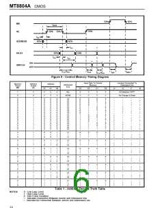
AC Electrical Characteristics† - Control and I/O Timings- Voltages are with respect to VSS=VEE=0V unless
otherwise stated.
‡
Characteristics
Sym
Min
Typ
Max Units
Test Conditions
=10V
1
2
Digital Input Capacitance
Setup Time D0-D3 to AE
C
5
pF
V
DI
DD
t
150
200
ns
ns
V
V
=10V
=5V
DS
DD
DD
3
4
5
6
7
8
9
Hold Time D0-D3 to AE
Setup Time Address to AE
Hold Time Address to AE
AE Pulse Width
t
120
300
ns
ns
V
V
=10V
=5V
DH
DD
DD
t
0
50
ns
ns
V
V
=10V
=5V
AS
AH
DD
DD
t
120
300
ns
ns
V
V
=10V
=5V
DD
DD
t
100
250
ns
ns
V
V
=10V
=5V
AEW
DD
DD
AE to Switch Status Delay
DATA to Switch Status Delay
MR to Switch Status Delay
t
200
650
300
900
ns
ns
V
V
=10V
=5V
PAE
DD
DD
See Note 1
See Note 1
t
t
250
650
400
1000
ns
ns
V
V
=10V
=5V
PLH
PHL
DD
DD
t
250
500
200
500
400
600
350
750
ns
ns
ns
ns
V
V
V
V
=10V
=5V
=10V
=5V
MR
DD
DD
DD
DD
See Note 2
t
MRR
† AC Electrical Characteristics are at ambient temperature (25°C).
‡ Typical figures are for design aid only; not guaranteed and not subject to production testing.
Note 1 RL= 10kΩ, CL=50pF
Note 2 RL= 1kΩ, CL=50pF
Digital Input rise time (tr) and fall time (tf) = 5ns.
3-7

 MITEL [ MITEL NETWORKS CORPORATION ]