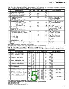
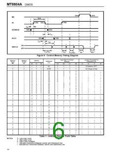
MT8804A CMOS
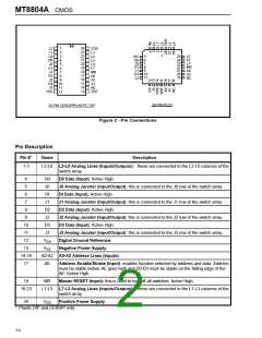
24
23
22
21
20
19
18
17
16
15
14
13
1
2
3
4
5
6
7
8
L2
L1
L0
D0
J0
D1
J1
D2
J2
D3
J3
VDD
L3
L4
L5
L6
•
NC
L5
5
25
24
23
22
21
20
19
L6
6
D0
7
L7
J0
D1
J1
8
MR
AE
A2
NC
L7
9
MR
AE
A2
A1
A0
D2
J2
10
11
9
10
11
12
VSS
VEE
28 PIN PLCC
24 PIN CERDIP/PLASTIC DIP
Figure 2 - Pin Connections
Pin Description
Pin #*
Name
Description
1-3
L2-L0 L2-L0 Analog Lines (Inputs/Outputs): these are connected to the L2-L0 columns of the
switch array.
4
5
D0
J0
DI
D0 Data (Input): Active High.
J0 Analog Junctor (Input/Output): this is connected to the J0 row of the switch array.
DI Data (Input). Active High.
6
7
J1
D2
J2
D3
J3
J1 Analog Junctor (Input/Output): this is connected to the J1 row of the switch array.
D2 Data (Input): Active High.
8
9
J2 Analog Junctor (Input/Output): this is connected to the J2 row of the switch array.
D3 Data (Input): Active High.
10
11
12
13
14-16
17
J3 Analog Junctor (Input/Output): this is connected to the J3 row of the switch array.
Digital Ground Reference.
V
SS
EE
V
Negative Power Supply.
A0-A2 A0-A2 Address Lines (Inputs).
AE
Address Enable/Strobe (Input): enables function selected by address and data. Address
must be stable before AE goes high and D0-D3 must be stable on the falling edge of the
AE. Active High.
18
MR
Master RESET (Input): this is used to turn off all switches. Active High.
19-23
L7-L3 L7-L3 Analog Lines (Inputs/Outputs): these are connected to the L7-L3 columns of the
switch array.
24
V
Positive Power Supply.
DD
* Plastic DIP and CERDIP only
3-4

 MITEL [ MITEL NETWORKS CORPORATION ]