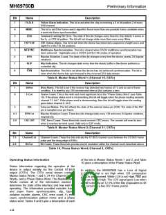
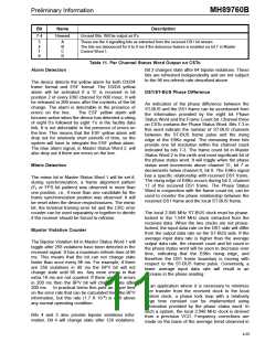
MH89760B
Preliminary Information
the phase status word. For example, if the channel
count in the phase status word is seen to increase
over time, the feedback applied to the VCO is used
to decrease the system clock frequency until a
reversal in the trend is observed.
kHz signal is output at the E8Ko pin and can be used
to phase lock the local system C2 and the transmit
C1.5 clocks to the extracted clock.
The MH89760B requires three clock signals which
have to be generated externally.
The ST-BUS
The elastic buffer in the MH89760B permits the
device to handle eight channels of jitter/wander (see
description of elastic buffer in the next section). In
order to prevent slips from occurring, the frequency
corrections would have to be implemented such that
the deviation in the phase status word is limited to
eight channels peak to peak. It is possible to use a
more sophisticated protocol which would center the
elastic buffer and permit more jitter/wander to be
handled. However, for most applications, the eight
channels of jitter/wander tolerance is acceptable.
interface on the device requires a 2.048 MHz signal
which is applied at the C2i pin and an 8
kHz framing signal applied at the F0i pin.
The
framing signal is used to delimit individual ST-
BUS frames. Figure 19 illustrates the relationship
between the C2i and F0i signals. The F0i signal can
be derived from the 2.048 MHz C2 clock. The
transmit side of the DS1 interface requires a 1.544
MHz clock applied at C1.5i. The C1.5 and C2 clocks
must be phase locked. There must be 193 clock
cycles of the C1.5 clock for every 256 cycles of the
C2 clock in order for the 2.048 to 1.544 rate
converter to function properly.
Received Signalling Bits
In synchronous operation the slave end of the link
must have its C2 and C1.5 clocks phase locked to
the extracted clock. In plesiochronous clocking
applications where the master and slave end are
operating under controlled slip conditions, phase
locking to the extracted clock is generally not
required.
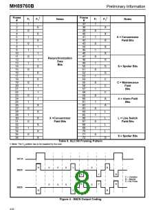
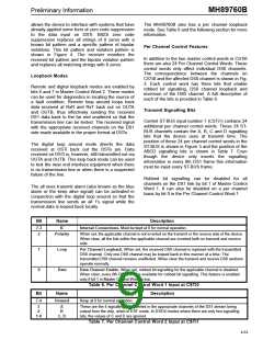
The A, B, C and D signalling bits are output from the
device in the 24 Per Channel Status Words. Their
location in the serial steam output at CSTo is shown
in Figure 3 and the bit positions are shown in Table
11. The internal debouncing of the signalling bits
can be turned on or off by Master Control Word 1. In
ESF mode, A, B, C and D bits are valid. Even
though the signalling bits are only received once
every six frames the device stores the information so
that it is available on the ST-BUS every frame. The
ST-BUS will always contain the most recent
signalling bits. The state of the signalling bits is
frozen if synchronization is lost.
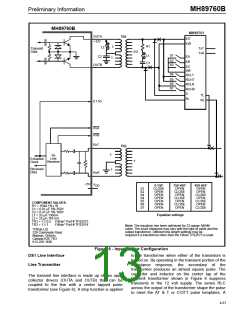
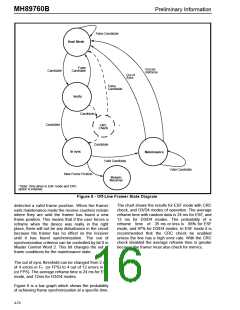
Mitel’s MT8941 Digital Phase Lock Loop (DPLL) can
be used to generate all timing signals required by the
MH89760B. The MT8941 has two DPLLs built into
the device. Figure 5 shows how DPLL #1 can be set
up to generate the C1.5 clock phase locked to the
F0i which in turn is derived from the same source
as the C2 clock.
Figure 5 also shows how DPLL
In D3/D4 mode, only the A and B bits are valid. The
state of the signalling bits is frozen when terminal
frame synchronization is lost. The freeze is disabled
#2 is set up to generate the ST-BUS clocks that are
phase locked to the received data rate. If E8Ko from
the MH89760B is connected to the C8Kb input on
the MT8941, DPLL #2 in the device will generate the
ST-BUS clocks that are phase locked to the T1 line.
when
the
device
regains
terminal
frame
synchronization. The signalling bits may go through
a random transition stage until the device attains
multiframe synchronization.
MT8941
DPLL #1
Clock and Framing Signals
CVb
F0i
C12i
C1.5
+5V
ENCv
The MH89760B has a built in clock extraction circuit
which creates a 1.544 MHz clock synchronized to
MS1
the received DS1 signal.
internally by the MH89760B to clock in data
received on RxT and RxR, and is also output at the
This clock is used
DPLL #2
F0b
C4b
C8Kb
C16i
MS0
F0i
C4i
E1.5o pin.
The circuit has been designed to
C2o
C2i
operate within the constraints imposed by the
minimum 1’s density requirements, typically
specified for T1 networks (maximum of 15
consecutive 0’s).
ENC4o
+5V
5V
MS2
MS3
ENC2o
Ai
Bi
Yo
The extracted clock is internally divided by 193 and
aligned with the received DS1 frame. The resulting 8
Figure 5 - MT8941 Clock Generator
4-66

 MITEL [ MITEL NETWORKS CORPORATION ]