MH88620BR
Preliminary Information
1
2
3
4
5
6
7
8
21
22
23
24
25
26
27
28
29
30
31
32
33
34
35
36
37
38
39
40
TIP
RING
TF1
TF2
RF1
RF2
LGND
LCA
VBAT
IC
RGND
VRLY
RRD
RNGC
REVC
ESI
N2
NC
Z1
Z2
TX
RX
GTX0
GTX1
GRX0
GRX1
NC
NC
NC
SHK
IC
IC
9
10
11
12
13
14
15
16
17
18
19
20
ESE
IC
IC
VEE
VDD
AGND
NATT
N1
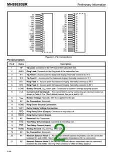
Figure 2 - Pin Connections
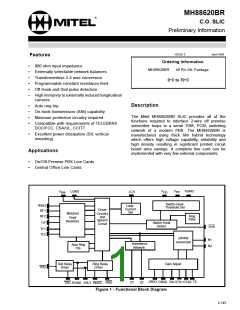
Description
Pin Description
Pin #
Name
1
2
3
4
5
6
7
8
TIP
RING
TF1
Tip Lead. Connects to the TIP lead of the subscriber line.
Ring Lead: Connects to the Ring lead of the subscriber line.
Tip Feed 1: Access point for balanced ringing. Normally connects to TF2.
Tip Feed 2: Access point for balanced ringing. Normally connects to TF1.
Ring Feed 1: Access point for balanced ringing. Normally connects to RF2.
Ring Feed 2: Access point for balanced ringing. Normally connects to RF1.
TF2
RF1
RF2
LGND Battery Ground. VBat return path. Connected to system’s energy dumping ground.
LCA
Current Limit Set (Input): The current limit is set by connecting an external resistor as
shown in Table 5. For 70mA default current, this pin is tied to -5V.
9
VBat
NC
Battery Voltage: Typically -48V dc is applied to this pin.
No Connection: Reserved.
10
11
12
13
14
15
16
17
18
19
20
RGND Ring Driver Ground Connection.
VRLY
RRD
Relay Supply Voltage Connection.
Ring Relay Drive (Output). Connects to ring relay coil.
RNGC Ring Relay Control (Input) .
NC
Reserved. No Connection.
TRD
TRC
Test Relay Drive (Output): Connects to test relay coil.
Test Relay Control (Input).
AGND Analog Ground: VDD and VEE return path.
.
NC
N1
No Connection: Reserved.
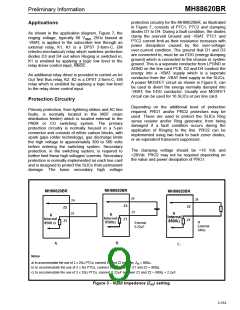
Network Balance Node 1. An external network balance impedance can be connected
between N1 and AGND. See Fig 4. For complex impedances N2 no connection.
21
N2
Network Balance Node 2. An external network balance impedance can be connected
between N2 and AGND. See Fig 4 N2 connects to GND for 900Ω balance.
2-146

 MITEL [ MITEL NETWORKS CORPORATION ]