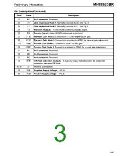
Preliminary Information
MH88620BR
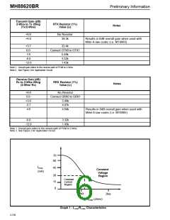
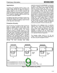
bias voltage. The loop current is proportional to this
voltage. The loop current can be set between 20 and
70 mA by various connections to the LCA pin as
illustrated in Table 5 and Figure 5. The loop current
during a fault condition will be limited to the constant
loop current programmed. Primary over current
protection is inherent in the current limiting feature of
the 200 ohm battery feed resistor. Refer to Graph 1.
Functional Description
The SLIC uses a transformerless electronic 2-4 wire
converter which can be connected to a Codec to
interface the 2 wire subscriber loops to a time
division multiplexed (TDM) pulse code modulated
(PCM) digital switching network. For analog
applications, the TXRX of the 2 wire converter can
be connected directly to an analog crosspoint switch,
such as the MT8816. Powering of the line is provided
through precision battery feed resistors. The
MH88620BR also contains control, signalling and
status circuitry solution which combines to provide
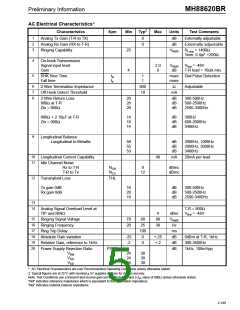
Receive and Transmit Audio Path
The audio signal of the 2-wire is sensed differentially
across the 200 ohm feed resistor and is passed on to
a second differential amplifier stage in the 2W/4W
conversion block. This block sets the transmit gain
on the 4-wire side and cancels signals originating
from the receive input.
a
complete functional solution, simplifying the
manufacture of line cards. This circuitry is illustrated
in the functional block diagram in Fig 1. The
MH88620BR is designed to be pin compatible with
Mitel’s MH88632, MH88625 and MH88628. This
allows a common PCB design with common gain,
input impedance and network balance.
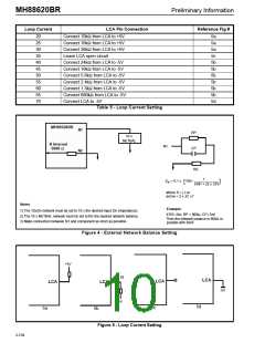
Programmable Transmit and Receive Gain
Transmit Gain (Tip-Ring to Tx) and Receive Gain (Rx
to Tip-Ring) are programmed by connecting external
resistors (RRX and RTX) from GRX1 to AGND and
from GTX1 to AGND as indicated in Figure 2 and
Table 1 and 2. The programmable gain range is from
-12dB to +6dB; this wide range will accommodate
any loss plan. Alternatively, the default Receive Gain
of 0dB and Transmit Gain of 0dB can be obtained by
connecting GRX0 to GRX1 and GTX0 to GTX1. In
addition, a Receive Gain of +6dB and Transmit Gain
of +6dB can be obtained by not connecting resistors
RRX and RTX. For correct gain programming. the
MH88620BR’s Tip-Ring impedance (Zin) must match
the line termination impedance.
Approvals
FCC part 68, CCITT, DOS CS-03, UL 1459, CAN/
CSA-22.2 N0. 225-M90 and ANSI/EIA/TIA-464-A are
system level safety standards and performance
requirements. As a component of a system, the
MH88620BR is designed to comply with the
applicable requirements of these specifications.
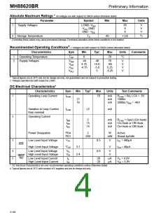
Battery Feed
The loop current for the subscriber equipment is
sourced through a pair of matched 200 ohm resistors
connected to the TIP and RING. The two wire loop is
biased such that the Ring lead is 2V above VBAT
(typically -46V) and the TIP lead is 2V below LGND
(typically -2V) during constant voltage mode.
For optimum performance, resistors RRX should be
physically located as close as possible to the GRX1
input pin, and resistor RTX should be physically
located as close as possible to the GTX1 input pin.
The SLIC is designed for a nominal battery voltage
of -48Vdc and can provide the maximum loop current
of 70mA under this condition.
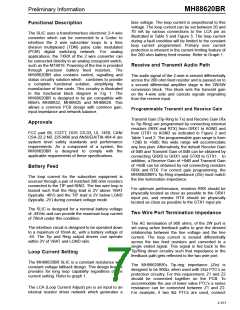
Two Wire Port Termination Impedance
The AC termination of 900 ohms, of the 2W port is
set using active feedback paths to give the desired
relationship between the line voltage and the line
current. The loop current is sensed differentially
across the two feed resistors and converted to a
single ended signal. This signal is fed back to the
Tip/Ring driver circuitry such that impedance in the
feedback path gets reflected to the two wire port.
The interface circuit is designed to be operated down
to a maximum of 16mA dc, with a battery voltage of
-44. The Tip and Ring output drivers can operate
within 2V of VBAT and LGND rails.
Loop Current Setting
The MH88620BR SLIC is a constant resistance with
constant voltage fallback design. This design feature
provides for long loop capability regardless of the
current setting. Refer to graph 1.
The MH88620BR’s Tip-ring impedance (Zin) is
designed to be 900Ω, when used with 25Ω PTC’s as
protection circuitry. For this requirement, Z1 and Z2
should be connected together on the PCB. To
accommodate the use of lower value PTC’s a series
resistance can be connected between Z1 and Z2.
For example, it two 8Ω PTCs are used, connect
The LCA (Loop Current Adjust) pin is an input to an
internal resistor driver network which generates a
2-151

 MITEL [ MITEL NETWORKS CORPORATION ]