ADVANCE
128Mb: x16, x32
MOBILE SDRAM
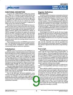
128Mb SDRAM PART NUMBERS
PART NUMBER
VDD/VDDQ
ARCHITECTURE
8 Meg x 16
8 Meg x 16
4 Meg x 32
4 Meg x 32
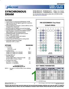
PACKAGE
54-BALL VFBGA
54-BALL VFBGA
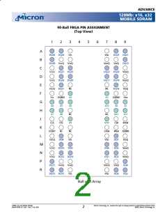
90-BALL FBGA
90-BALL FBGA
MT48LC8M16LFFF-xx
MT48V8M16LFFF-xx
MT48LC4M32LFFC-xx
MT48V4M32LFFC-xx
3.3V / 3.3V
2.5V / 2.5V-1.8V
3.3V / 3.3V
2.5V / 2.5V-1.8V
GENERAL DESCRIPTION
®
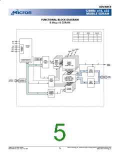
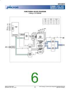
The Micron 128Mb SDRAM is a high-speed CMOS,
dynamicrandom-accessmemorycontaining134,217,728
bits. It is internally configured as a quad-bank DRAM
withasynchronousinterface(allsignalsareregisteredon
the positive edge of the clock signal, CLK). Each of the
x16’s 33,554,432-bit banks is organized as 4,096 rows by
512 columns by 16 bits. Each of the x32’s 33,554,432-bit
banks is organized as 4,096 rows by 256 columns by 32
bits.
precharge that is initiated at the end of the burst se-
quence.
The 128Mb SDRAM uses an internal pipelined
architecture to achieve high-speed operation. This
architecture is compatible with the 2n rule of prefetch
architectures, but it also allows the column address to be
changed on every clock cycle to achieve a high-speed,
fully random access. Precharging one bank while access-
ing one of the other three banks will hide the precharge
cycles and provide seamless high-speed, random-access
operation.
The 128Mb SDRAM is designed to operate in 3.3V or
2.5V, low-power memory systems. An auto refresh mode
is provided, along with a power-saving, power-down
mode. All inputs and outputs are LVTTL-compatible.
SDRAMs offer substantial advances in DRAM operat-
ing performance, including the ability to synchronously
burst data at a high data rate with automatic column-
address generation, the ability to interleave between in-
ternal banks in order to hide precharge time and the
capabilitytorandomlychangecolumnaddressesoneach
clock cycle during a burst access.
Read and write accesses to the SDRAM are burst ori-
ented; accesses start at a selected location and continue
for a programmed number of locations in a programmed
sequence. Accesses begin with the registration of an AC-
TIVE command, which is then followed by a READ or
WRITE command. The address bits registered coinci-
dent with the ACTIVE command are used to select the
bank and row to be accessed (BA0, BA1 select the bank;
A0-A11 select the row). The address bits registered coin-
cident with the READ or WRITE command are used to
select the starting column location for the burst access.
The SDRAM provides for programmable READ or
WRITE burst lengths of 1, 2, 4, or 8 locations, or the full
page, with a burst terminate option. An auto precharge
function may be enabled to provide a self-timed row
128Mb: x16, x32 Mobile SDRAM
MobileY95W_3V_F.p65 – Rev. F; Pub. 9/02
Micron Technology, Inc., reserves the right to change products or specifications without notice.
©2002, Micron Technology, Inc.
3

 MICRON [ MICRON TECHNOLOGY ]