1Gb: x4, x8, x16 DDR2 SDRAM
Input Slew Rate Derating
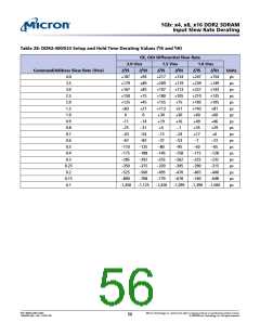
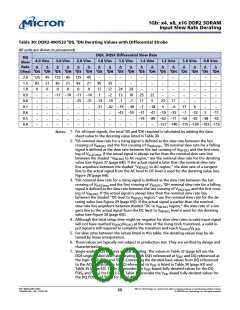
Table 30: DDR2-400/533 tDS, tDH Derating Values with Differential Strobe
All units are shown in picoseconds
DQS, DQS# Differential Slew Rate
1.8 V/ns 1.6 V/ns 1.4 V/ns
DQ
Slew
Rate
4.0 V/ns
3.0 V/ns
2.0 V/ns
1.2 V/ns
1.0 V/ns
0.8 V/ns
Δ
Δ
Δ
Δ
Δ
Δ
Δ
Δ
Δ
Δ
Δ
Δ
Δ
Δ
Δ
Δ
Δ
Δ
(V/ns) tDS tDH tDS tDH tDS tDH tDS tDH tDS tDH tDS tDH tDS tDH tDS tDH tDS tDH
2.0
1.5
1.0
0.9
0.8
0.7
0.6
0.5
0.4
125
83
0
45
21
0
125
83
0
45
21
0
125
83
0
45
21
0
–
–
–
–
–
–
–
–
–
–
–
–
–
–
–
–
–
–
–
–
–
–
5
–
–
95
12
1
33
12
–2
–
–
24
13
–1
24
10
–7
–
–
–
–
–
–
–
–11 –14 –11 –14
25
11
–7
22
5
–
–
–
–
–
–
–
–25 –31 –13 –19
23
5
17
–6
–
–
–
–
–
–
–
–
–
–
–
–
–
–
–
–31 –42 –19 –30
–18
17
–7
6
–
–
–
–
–
–
–
–
–
–
–
–43 –59 –31 –47 –19 –35
–23
–11
–
–
–
–
–
–
–
–
–74 –89 –62 –77 –50 –65 –38 –53
–127 –140 –115 –128 –103 –116
–
–
–
–
–
–
–
–
–
–
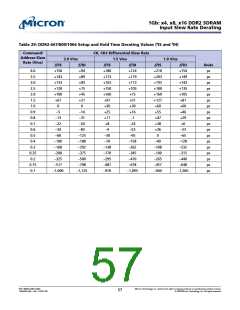
1. For all input signals, the total tDS and tDH required is calculated by adding the data
sheet value to the derating value listed in Table 30.
Notes:
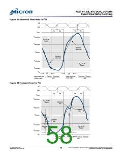
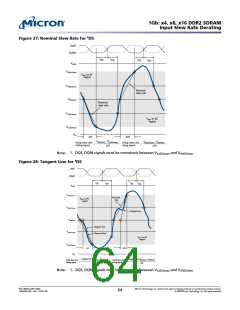
2. tDS nominal slew rate for a rising signal is defined as the slew rate between the last
crossing of VREF(DC) and the first crossing of VIH(AC)min. tDS nominal slew rate for a falling
signal is defined as the slew rate between the last crossing of VREF(DC) and the first cross-
ing of VIL(AC)max. If the actual signal is always earlier than the nominal slew rate line
between the shaded “VREF(DC) to AC region,” use the nominal slew rate for the derating
value (see Figure 27 (page 64)). If the actual signal is later than the nominal slew rate
line anywhere between the shaded “VREF(DC) to AC region,” the slew rate of a tangent
line to the actual signal from the AC level to DC level is used for the derating value (see
Figure 28 (page 64)).
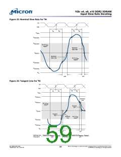
3. tDH nominal slew rate for a rising signal is defined as the slew rate between the last
crossing of VIL(DC)max and the first crossing of VREF(DC). tDH nominal slew rate for a falling
signal is defined as the slew rate between the last crossing of VIH(DC)min and the first cross-
ing of VREF(DC). If the actual signal is always later than the nominal slew rate line
between the shaded “DC level to VREF(DC) region,” use the nominal slew rate for the de-
rating value (see Figure 29 (page 65)). If the actual signal is earlier than the nominal
slew rate line anywhere between shaded “DC to VREF(DC) region,” the slew rate of a tan-
gent line to the actual signal from the DC level to VREF(DC) level is used for the derating
value (see Figure 30 (page 65)).
4. Although the total setup time might be negative for slow slew rates (a valid input signal
will not have reached VIH[AC]/VIL[AC] at the time of the rising clock transition), a valid in-
put signal is still required to complete the transition and reach VIH(AC)/VIL(AC)
.
5. For slew rates between the values listed in this table, the derating values may be ob-
tained by linear interpolation.
6. These values are typically not subject to production test. They are verified by design and
characterization.
7. Single-ended DQS requires special derating. The values in Table 32 (page 62) are the
DQS single-ended slew rate derating with DQS referenced at VREF and DQ referenced at
the logic levels tDSb and tDHb. Converting the derated base values from DQ referenced
to the AC/DC trip points to DQ referenced to VREF is listed in Table 34 (page 63) and
Table 35 (page 63). Table 34 provides the VREF-based fully derated values for the DQ
(tDSa and tDHa) for DDR2-533. Table 35 provides the VREF-based fully derated values for
the DQ (tDSa and tDHa) for DDR2-400.
PDF: 09005aef821ae8bf
1GbDDR2.pdf – Rev. T 02/10 EN
Micron Technology, Inc. reserves the right to change products or specifications without notice.
60
© 2004 Micron Technology, Inc. All rights reserved.

 MICRON [ MICRON TECHNOLOGY ]