1Gb: x4, x8, x16 DDR2 SDRAM
AC Overshoot/Undershoot Specification
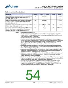
Table 27: AC Input Test Conditions
Parameter
Symbol
Min
Max
Units
Notes
Input setup timing measurement reference level address
balls, bank address balls, CS#, RAS#, CAS#, WE#, ODT,
DM, UDM, LDM, and CKE
VRS
See Note 2
1, 2, 3, 4
Input hold timing measurement reference level address
balls, bank address balls, CS#, RAS#, CAS#, WE#, ODT,
DM, UDM, LDM, and CKE
VRH
See Note 5
1, 3, 4, 5
Input timing measurement reference level (single-ended)
DQS for x4, x8; UDQS, LDQS for x16
VREF(DC)
VRD
VDDQ × 0.49 VDDQ × 0.51
VIX(AC)
V
V
1, 3, 4, 6
Input timing measurement reference level (differential)
CK, CK# for x4, x8, x16; DQS, DQS# for x4, x8; RDQS,
RDQS# for x8; UDQS, UDQS#, LDQS, LDQS# for x16
1, 3, 7, 8, 9
1. All voltages referenced to VSS.
Notes:
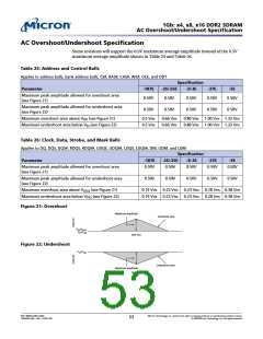
2. Input waveform setup timing (tISb) is referenced from the input signal crossing at the
VIH(AC) level for a rising signal and VIL(AC) for a falling signal applied to the device under
test, as shown in Figure 31 (page 66).
3. See Input Slew Rate Derating (page 55).
4. The slew rate for single-ended inputs is measured from DC level to AC level, VIL(DC) to
VIH(AC) on the rising edge and VIL(AC) to VIH(DC) on the falling edge. For signals referenced
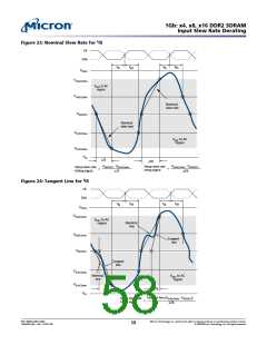
to VREF, the valid intersection is where the “tangent” line intersects VREF, as shown in
Figure 24 (page 58), Figure 26 (page 59), Figure 28 (page 64), and Figure 30
(page 65).
5. Input waveform hold (tIHb) timing is referenced from the input signal crossing at the
VIL(DC) level for a rising signal and VIH(DC) for a falling signal applied to the device under
test, as shown in Figure 31 (page 66).
6. Input waveform setup timing (tDS) and hold timing (tDH) for single-ended data strobe is
referenced from the crossing of DQS, UDQS, or LDQS through the Vref level applied to
the device under test, as shown in Figure 33 (page 67).
7. Input waveform setup timing (tDS) and hold timing (tDH) when differential data strobe
is enabled is referenced from the cross-point of DQS/DQS#, UDQS/UDQS#, or LDQS/
LDQS#, as shown in Figure 32 (page 66).
8. Input waveform timing is referenced to the crossing point level (VIX) of two input signals
(VTR and VCP) applied to the device under test, where VTR is the true input signal and VCP
is the complementary input signal, as shown in Figure 34 (page 67).
9. The slew rate for differentially ended inputs is measured from twice the DC level to
twice the AC level: 2 × VIL(DC) to 2 × VIH(AC) on the rising edge and 2 × VIL(AC) to 2 ×
VIH(DC) on the falling edge. For example, the CK/CK# would be –250mV to +500mV for
CK rising edge and would be +250mV to –500mV for CK falling edge.
PDF: 09005aef821ae8bf
1GbDDR2.pdf – Rev. T 02/10 EN
Micron Technology, Inc. reserves the right to change products or specifications without notice.
54
© 2004 Micron Technology, Inc. All rights reserved.

 MICRON [ MICRON TECHNOLOGY ]