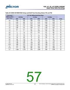
1Gb: x4, x8, x16 DDR2 SDRAM
AC Overshoot/Undershoot Specification
AC Overshoot/Undershoot Specification
Some revisions will support the 0.9V maximum average amplitude instead of the 0.5V
maximum average amplitude shown in Table 25 and Table 26.
Table 25: Address and Control Balls
Applies to address balls, bank address balls, CS#, RAS#, CAS#, WE#, CKE, and ODT
Specification
-3/-3E
Parameter
-187E
-25/-25E
-37E
-5E
Maximum peak amplitude allowed for overshoot area
(see Figure 21)
0.50V
0.50V
0.50V
0.50V
0.50V
0.50V
Maximum peak amplitude allowed for undershoot area
(see Figure 22)
0.50V
0.50V
0.50V
0.50V
Maximum overshoot area above VDD (see Figure 21)
Maximum undershoot area below VSS (see Figure 22)
0.5 Vns
0.5 Vns
0.66 Vns
0.66 Vns
0.80 Vns 1.00 Vns 1.33 Vns
0.80 Vns 1.00 Vns 1.33 Vns
Table 26: Clock, Data, Strobe, and Mask Balls
Applies to DQ, DQS, DQS#, RDQS, RDQS#, UDQS, UDQS#, LDQS, LDQS#, DM, UDM, and LDM
Specification
-3/-3E
Parameter
-187E
-25/-25E
-37E
-5E
Maximum peak amplitude allowed for overshoot area
(see Figure 21)
0.50V
0.50V
0.50V
0.50V
0.50V
Maximum peak amplitude allowed for undershoot area
(see Figure 22)
0.50V
0.50V
0.50V
0.50V
0.50V
Maximum overshoot area above VDDQ (see Figure 21)
Maximum undershoot area below VSSQ (see Figure 22)
0.19 Vns
0.19 Vns
0.23 Vns
0.23 Vns
0.23 Vns
0.23 Vns
0.28 Vns 0.38 Vns
0.28 Vns 0.38 Vns
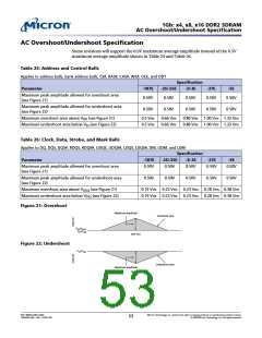
Figure 21: Overshoot
Maximum amplitude
Overshoot area
VDD/VDDQ
VSS/VSSQ
Time (ns)
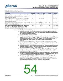
Figure 22: Undershoot
VSS/VSSQ
Undershoot area
Maximum amplitude
Time (ns)
PDF: 09005aef821ae8bf
1GbDDR2.pdf – Rev. T 02/10 EN
Micron Technology, Inc. reserves the right to change products or specifications without notice.
53
© 2004 Micron Technology, Inc. All rights reserved.

 MICRON [ MICRON TECHNOLOGY ]