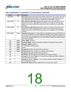
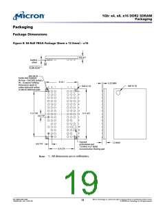
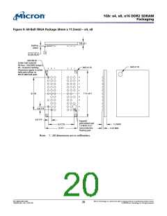
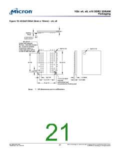
1Gb: x4, x8, x16 DDR2 SDRAM
Packaging
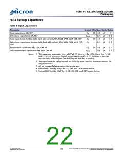
FBGA Package Capacitance
Table 4: Input Capacitance
Parameter
Symbol Min Max Units Notes
Input capacitance: CK, CK#
CCK
CDCK
CI
1.0 2.0
0.25 pF
1.0 2.0 pF
0.25 pF
pF
1
Delta input capacitance: CK, CK#
2, 3
1, 4
2, 3
–
Input capacitance: Address balls, bank address balls, CS#, RAS#, CAS#, WE#, CKE, ODT
Delta input capacitance: Address balls, bank address balls, CS#, RAS#, CAS#, WE#, CKE,
ODT
CDI
–
Input/output capacitance: DQ, DQS, DM, NF
CIO
2.5 4.0
0.5
pF
pF
1, 5
2, 3
Delta input/output capacitance: DQ, DQS, DM, NF
CDIO
–
1. This parameter is sampled. VDD = +1.8V ±0.1V, VDDQ = +1.8V ±0.1V, VREF = VSS, f = 100
MHz, TC = 25°C, VOUT(DC) = VDDQ/2, VOUT (peak-to-peak) = 0.1V. DM input is grouped
with I/O balls, reflecting the fact that they are matched in loading.
Notes:
2. The capacitance per ball group will not differ by more than this maximum amount for
any given device.
3.
ΔC are not pass/fail parameters; they are targets.
4. Reduce MAX limit by 0.25pF for -25, -25E, and -187E speed devices.
5. Reduce MAX limit by 0.5pF for -3, -3E, -25, -25E, and -187E speed devices.
PDF: 09005aef821ae8bf
1GbDDR2.pdf – Rev. T 02/10 EN
Micron Technology, Inc. reserves the right to change products or specifications without notice.
© 2004 Micron Technology, Inc. All rights reserved.
22

 MICRON [ MICRON TECHNOLOGY ]