1 Mbit / 2 Mbit / 4 Mbit Multi-Purpose Flash
SST39SF010A / SST39SF020A / SST39SF040
Data Sheet
Product Description
The SST39SF010A/020A/040 are CMOS Multi-Purpose Flash (MPF) manufactured with SST’s propri-
etary, high performance CMOS SuperFlash technology. The split-gate cell design and thick oxide tun-
neling injector attain better reliability and manufacturability compared with alternate approaches. The
SST39SF010A/020A/040 devices write (Program or Erase) with a 4.5-5.5V power supply. The
SST39SF010A/020A/040 devices conform to JEDEC standard pinouts for x8 memories.
Featuring high performance Byte-Program, the SST39SF010A/020A/040 devices provide a maximum
Byte-Program time of 20 µsec. These devices use Toggle Bit or Data# Polling to indicate the comple-
tion of Program operation. To protect against inadvertent write, they have on-chip hardware and Soft-
ware Data Protection schemes. Designed, manufactured, and tested for a wide spectrum of
applications, these devices are offered with a guaranteed typical endurance of 100,000 cycles. Data
retention is rated at greater than 100 years.
The SST39SF010A/020A/040 devices are suited for applications that require convenient and econom-
ical updating of program, configuration, or data memory. For all system applications, they significantly
improve performance and reliability, while lowering power consumption. They inherently use less
energy during erase and program than alternative flash technologies. The total energy consumed is a
function of the applied voltage, current, and time of application. Since for any given voltage range, the
SuperFlash technology uses less current to program and has a shorter erase time, the total energy
consumed during any Erase or Program operation is less than alternative flash technologies. These
devices also improve flexibility while lowering the cost for program, data, and configuration storage
applications.
The SuperFlash technology provides fixed Erase and Program times, independent of the number of
Erase/Program cycles that have occurred. Therefore the system software or hardware does not have
to be modified or de-rated as is necessary with alternative flash technologies, whose Erase and Pro-
gram times increase with accumulated Erase/Program cycles.
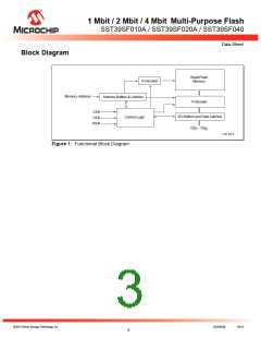
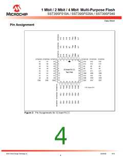
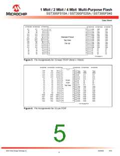
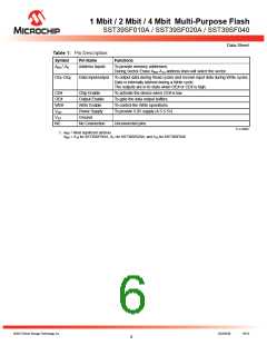
To meet high density, surface mount requirements, the SST39SF010A/020A/040 are offered in 32-lead
PLCC and 32-lead TSOP packages. A 600 mil, 32-pin PDIP is also available. See Figures 2, 3, and 4
for pin assignments.
©2013 Silicon Storage Technology, Inc.
DS25022B
04/13
2

 MICROCHIP [ MICROCHIP ]