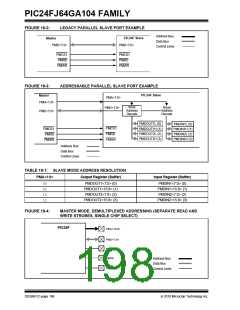
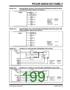
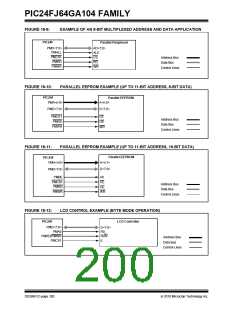
PIC24FJ64GA104 FAMILY
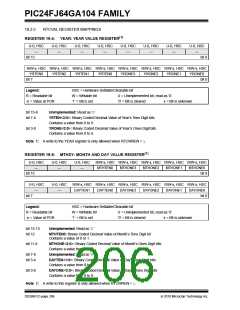
TABLE 19-2: ALRMVAL REGISTER
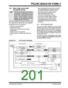
19.2 RTCC Module Registers
MAPPING
The RTCC module registers are organized into three
categories:
Alarm Value Register Window
ALRMPTR
<1:0>
• RTCC Control Registers
• RTCC Value Registers
• Alarm Value Registers
ALRMVAL<15:8> ALRMVAL<7:0>
00
01
10
11
ALRMMIN
ALRMWD
ALRMMNTH
—
ALRMSEC
ALRMHR
ALRMDAY
—
19.2.1
REGISTER MAPPING
To limit the register interface, the RTCC Timer and
Alarm Time registers are accessed through
corresponding register pointers. The RTCC Value
register window (RTCVALH and RTCVALL) uses the
RTCPTR bits (RCFGCAL<9:8>) to select the desired
Timer register pair (see Table 19-1).
Considering that the 16-bit core does not distinguish
between 8-bit and 16-bit read operations, the user must
be aware that when reading either the ALRMVALH or
ALRMVALL bytes, the ALRMPTR<1:0> value will be
decremented. The same applies to the RTCVALH or
RTCVALL bytes with the RTCPTR<1:0> being
decremented.
By writing to the RTCVALH byte, the RTCC Pointer
value (the RTCPTR<1:0> bits) decrements by one until
they reach ‘00’. Once they reach ‘00’, the MINUTES
and SECONDS value will be accessible through
RTCVALH and RTCVALL until the pointer value is
manually changed.
Note:
This only applies to read operations and
not write operations.
19.2.2
WRITE LOCK
TABLE 19-1: RTCVAL REGISTER MAPPING
To perform a write to any of the RTCC Timer registers,
the RTCWREN bit (RCFGCAL<13>) must be set (refer
to Example 19-1).
RTCC Value Register Window
RTCPTR<1:0>
RTCVAL<15:8> RTCVAL<7:0>
Note:
To avoid accidental writes to the timer, it is
recommended that the RTCWREN bit
(RCFGCAL<13>) is kept clear at any
other time. For the RTCWREN bit to be
set, there is only one instruction cycle time
window allowed between the 55h/AA
sequence and the setting of RTCWREN;
therefore, it is recommended that code
follow the procedure in Example 19-1.
00
01
10
11
MINUTES
WEEKDAY
MONTH
—
SECONDS
HOURS
DAY
YEAR
The Alarm Value register window (ALRMVALH and
ALRMVALL) uses the ALRMPTR bits
(ALCFGRPT<9:8>) to select the desired Alarm register
pair (see Table 19-2).
19.2.3
SELECTING RTCC CLOCK SOURCE
By writing to the ALRMVALH byte, the Alarm Pointer
value (ALRMPTR<1:0> bits) decrements by one until
they reach ‘00’. Once they reach ‘00’, the ALRMMIN
and ALRMSEC value will be accessible through
ALRMVALH and ALRMVALL until the pointer value is
manually changed.
The clock source for the RTCC module can be selected
using the Flash Configuration bit, RTCOSC (CW4<5>).
When the bit is set to ‘1’, the Secondary Oscillator
(SOSC) is used as the reference clock, and when the
bit is ‘0’, LPRC is used as the reference clock.
EXAMPLE 19-1:
SETTING THE RTCWREN BIT
asm volatile(“push w7”);
asm volatile(“push w8”);
asm volatile(“disi #5”);
asm volatile(“mov #0x55, w7”);
asm volatile(“mov w7, _NVMKEY”);
asm volatile(“mov #0xAA, w8”);
asm volatile(“mov w8, _NVMKEY”);
asm volatile(“bset _RCFGCAL, #13”);
asm volatile(“pop w8”);
//set the RTCWREN bit
asm volatile(“pop w7”);
DS39951C-page 202
2010 Microchip Technology Inc.

 MICROCHIP [ MICROCHIP ]