PIC24FJ64GA104 FAMILY
19.2.4
RTCC CONTROL REGISTERS
)
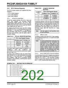
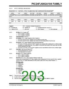
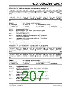
REGISTER 19-1: RCFGCAL: RTCC CALIBRATION AND CONFIGURATION REGISTER(1
R/W-0
RTCEN(2)
U-0
—
R/W-0
R-0, HSC
RTCSYNC HALFSEC(3)
R-0, HSC
R/W-0
R/W-0
R/W-0
RTCWREN
RTCOE
RTCPTR1
RTCPTR0
bit 15
bit 8
R/W-0
CAL7
R/W-0
CAL6
R/W-0
CAL5
R/W-0
CAL4
R/W-0
CAL3
R/W-0
CAL2
R/W-0
CAL1
R/W-0
CAL0
bit 7
bit 0
Legend:
HSC = Hardware Settable/Clearable bit
R = Readable bit
-n = Value at POR
W = Writable bit
‘1’ = Bit is set
U = Unimplemented bit, read as ‘0’
‘0’ = Bit is cleared x = Bit is unknown
bit 15
RTCEN: RTCC Enable bit(2)
1= RTCC module is enabled
0= RTCC module is disabled
bit 14
bit 13
Unimplemented: Read as ‘0’
RTCWREN: RTCC Value Registers Write Enable bit
1= RTCVALH and RTCVALL registers can be written to by the user
0= RTCVALH and RTCVALL registers are locked out from being written to by the user
bit 12
RTCSYNC: RTCC Value Registers Read Synchronization bit
1= RTCVALH, RTCVALL and ALCFGRPT registers can change while reading due to a rollover ripple
resulting in an invalid data read. If the register is read twice and results in the same data, the data
can be assumed to be valid.
0= RTCVALH, RTCVALL or ALCFGRPT registers can be read without concern over a rollover ripple
bit 11
bit 10
bit 9-8
HALFSEC: Half Second Status bit(3)
1= Second half period of a second
0= First half period of a second
RTCOE: RTCC Output Enable bit
1= RTCC output is enabled
0= RTCC output is disabled
RTCPTR<1:0>: RTCC Value Register Window Pointer bits
Points to the corresponding RTCC Value registers when reading the RTCVALH and RTCVALL registers.
The RTCPTR<1:0> value decrements on every read or write of RTCVALH until it reaches ‘00’.
RTCVAL<15:8>:
00= MINUTES
01= WEEKDAY
10= MONTH
11= Reserved
RTCVAL<7:0>:
00= SECONDS
01= HOURS
10= DAY
11= YEAR
Note 1: The RCFGCAL register is only affected by a POR.
2: A write to the RTCEN bit is only allowed when RTCWREN = 1.
3: This bit is read-only; it is cleared to ‘0’ on a write to the lower half of the MINSEC register.
2010 Microchip Technology Inc.
DS39951C-page 203

 MICROCHIP [ MICROCHIP ]